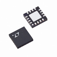
LTC3601EUD#PBF Linear Technology, LTC3601EUD#PBF Datasheet - Page 12

LTC3601EUD#PBF
Manufacturer Part Number
LTC3601EUD#PBF
Description
IC REG BUCK 1.5A ADJ 16QFN
Manufacturer
Linear Technology
Type
Step-Down (Buck)r
Datasheet
1.LTC3601EUDPBF.pdf
(26 pages)
Specifications of LTC3601EUD#PBF
Internal Switch(s)
Yes
Synchronous Rectifier
Yes
Number Of Outputs
1
Voltage - Output
0.5 ~ 14.52 V
Current - Output
1.5A
Frequency - Switching
800kHz ~ 4MHz
Voltage - Input
4 ~ 15 V
Operating Temperature
-40°C ~ 85°C
Mounting Type
Surface Mount
Package / Case
16-WQFN Exposed Pad
Lead Free Status / RoHS Status
Lead free / RoHS Compliant
Power - Output
-
Available stocks
Company
Part Number
Manufacturer
Quantity
Price
LTC3601
APPLICATIONS INFORMATION
highest capacitance density, but it is important to only
use types that have been surge tested for use in switching
power supplies. Aluminum electrolytic capacitors have
signifi cantly higher ESR but can be used in cost-sensitive
applications provided that consideration is given to ripple
current ratings and long-term reliability. Ceramic capacitors
have excellent low ESR characteristics and small footprints.
Their relatively low value of bulk capacitance may require
multiple capacitors in parallel.
Using Ceramic Input and Output Capacitors
Higher value, lower cost ceramic capacitors are now
available in small case sizes. Their high voltage rating
and low ESR make them ideal for switching regulator
applications. However, due to the self-resonant and high-Q
characteristics of some types of ceramic capacitors, care
must be taken when these capacitors are used at the input
and output. When a ceramic capacitor is used at the input,
and the power is supplied by a wall adapter through long
wires, a load step at the output can induce ringing at the
V
be mistaken as loop instability. At worst, a sudden inrush
of current through the long wires can potentially cause a
voltage spike at V
a more detailed discussion, refer to Application Note 88.
When choosing the input and output ceramic capacitors
choose the X5R or X7R dielectric formulations. These
dielectrics provide the best temperature and voltage
characteristics for a given value and size.
INTV
An internal low dropout (LDO) regulator produces a
3.3V supply voltage used to power much of the internal
LTC3601 circuitry including the power MOSFET gate
drivers. The INTV
regulator and must have a minimum of 1μF of decoupling
capacitance to ground. The decoupling capacitor should
have low impedance electrical connections to the INTV
and PGND pins to provide the transient currents required
by the LTC3601. The user may connect a maximum load
current of 5mA to this pin but must take into account the
increased power dissipation and die temperature that
12
IN
input. At best, this ringing can couple to the output and
CC
Regulator Bypass Capacitor
IN
CC
large enough to damage the part. For
pin connects to the output of this
CC
results. Furthermore, this supply is intended only to supply
additional DC load currents as desired and not intended
to regulate large transient or AC behavior this may impact
LTC3601 operation.
Boost Capacitor
The boost capacitor, C
above the applied input voltage V
capacitor is charged to a voltage equal to approximately
INTV
on. The charge on this capacitor is then used to supply
the required transient current during the remainder of the
switching cycle. When the top MOSFET is turned on, the
BOOST pin voltage will be equal to approximately V
3.3V. For most applications a 0.1μF ceramic capacitor will
provide adequate performance.
Output Voltage Programming
The LTC3601 will adjust the output voltage such that V
equals the reference voltage of 0.6V according to:
The desired output voltage is set by appropriate selection of
resistors R1 and R2 as shown in Figure 2. Choosing large
values for R1 and R2 will result in improved effi ciency but
may lead to undesirable noise coupling or phase margin
reduction due to stray capacitances at the FB node. Care
should be taken to route the FB line away from any noise
source, such as the SW line.
To improve the frequency response of the main control
loop a feedforward capacitor, C
in Figure 2.
V
OUT
CC
each time the bottom power MOSFET is turned
= 0.6V 1+
Figure 2. Optional Feedforward Capacitor
LTC3601
SGND
R2
R1
BOOST
FB
, is used to create a voltage rail
R1
R2
3601 F02
F
IN
, may be used as shown
. Specifi cally, the boost
C
F
V
OUT
3601fa
IN
FB
+


