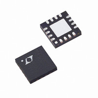
LTC3601EUD#PBF Linear Technology, LTC3601EUD#PBF Datasheet - Page 7

LTC3601EUD#PBF
Manufacturer Part Number
LTC3601EUD#PBF
Description
IC REG BUCK 1.5A ADJ 16QFN
Manufacturer
Linear Technology
Type
Step-Down (Buck)r
Datasheet
1.LTC3601EUDPBF.pdf
(26 pages)
Specifications of LTC3601EUD#PBF
Internal Switch(s)
Yes
Synchronous Rectifier
Yes
Number Of Outputs
1
Voltage - Output
0.5 ~ 14.52 V
Current - Output
1.5A
Frequency - Switching
800kHz ~ 4MHz
Voltage - Input
4 ~ 15 V
Operating Temperature
-40°C ~ 85°C
Mounting Type
Surface Mount
Package / Case
16-WQFN Exposed Pad
Lead Free Status / RoHS Status
Lead free / RoHS Compliant
Power - Output
-
Available stocks
Company
Part Number
Manufacturer
Quantity
Price
PIN FUNCTIONS
MODE/SYNC (Pin 1/Pin 15): Mode Selection and External
Synchronization Input Pin. This pin places the LTC3601
into forced continuous operation when tied to ground.
High effi ciency Burst Mode operation is enabled by either
fl oating this pin or by tying this pin to INTV
with an external clock, an internal phase-locked loop will
synchronize the phase and frequency of the internal oscil-
lator to that of the incoming clock signal. During external
clock synchronization, the LTC3601 will default to forced
continuous operation.
PGOOD (Pin 2/Pin 16): Open-Drain Power Good Output
Pin. PGOOD is pulled to ground when the voltage at the
FB pin is not within 8% (typical) of the internal 0.6V
reference. PGOOD becomes high impedance once the
voltage at the FB pin returns to within ±5% (typical) of
the internal reference.
SW (Pins 3, 4/Pins 1, 2): Switch Node Output Pin. Con-
nect this pin to the SW side of the external inductor. The
normal operation voltage swing of this pin ranges from
ground to PV
BOOST (Pin 6/Pin 5): Boosted Floating Driver Supply
Pin. The (+) terminal of the external bootstrap capacitor
connects to this pin while the (–) terminal connects to
the SW pin. The normal operation voltage swing of this
pin ranges from a diode voltage drop below INTV
to PV
INTV
This pin should be decoupled to PGND with a low ESR
ceramic capacitor of 1μF or more.
V
the voltage trip point for the on-time comparator. Connect
this pin to the regulated output to make the on-time pro-
portional to the output voltage when V
6V, switching frequency may become higher than the set
frequency. The pin impedance is normally 180kΩ.
SGND (Pin 9/Pin 17): Signal Ground Pin. This pin should
have a low noise connection to reference ground. The
feedback resistor network, external compensation network
and RT resistor should be connected to this ground. In
the MSE package, this pin must be soldered to the PCB
to provide a good thermal contact to the PCB.
ON
(Pin 8/Pin 7): On-Time Voltage Input Pin. This pin sets
CC
IN
(Pin 7/Pin 6): Internal 3.3V Regulator Output Pin.
+ INTV
IN
CC
.
.
(QFN/MSE)
OUT
CC
≤ 6V. If V
. When driven
CC
OUT
up
>
RT (Pin 10/Pin 8): Oscillator Frequency Program Pin. Con-
nect an external resistor, between 80k to 400k, from this
pin to SGND to program the LTC3601 switching frequency
from 800kHz to 4MHz. When RT is tied to INTV
switching frequency will default to 2MHz.
FB (Pin 11/Pin 9): Output Voltage Feedback Pin. Input to
the error amplifi er that compares the feedback voltage to
the internal 0.6V reference voltage. Connect this pin to
the appropriate resistor divider network to program the
desired output voltage.
ITH (Pin 12/Pin 10): Error Amplifi er Output and Switching
Regulator Compensation Pin. Connect this pin to appro-
priate external components to compensate the regulator
loop frequency response. Connect this pin to INTV
use the default internal compensation.
TRACK (Pin 13/Pin 11): Output Voltage Tracking and Soft-
Start Input Pin. Forcing a voltage below 0.6V on this pin
overrides the internal reference input to the error amplifi er.
The LTC3601 will servo the FB pin to the TRACK voltage
under this condition. Above 0.6V, the tracking function
stops and the internal reference resumes control of the
error amplifi er. An internal 1.4μA pull-up current from
INTV
by connecting an external capacitor between this pin and
ground. See Applications Information section for more
details.
RUN (Pin 14/Pin 12): Regulator Enable Pin. Enables chip
operation by applying a voltage above 1.25V. A voltage
below 1V on this pin places the part into shutdown. Do
not fl oat this pin.
V
Pins. These pins should be closely decoupled to PGND
with a low ESR capacitor of 10μF or more.
PGND (Pin 17/Pins 3, 4): Power Ground Pin. The (–)
terminal of the input bypass capacitor, C
terminal of the output capacitor, C
this pin with a low impedance connection. In the QFN
package this pin must be soldered to the PCB to provide
low impedance electrical contact to ground and good
thermal contact to the PCB.
IN
(Pins 15, 16/Pins 13, 14): Main Power Supply Input
CC
allows a soft-start function to be implemented
OUT
, should be tied to
LTC3601
IN
, and the (–)
CC
CC
, the
3601fa
7
to


