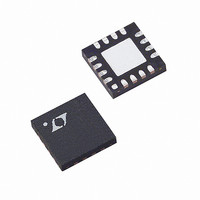
LTC3601EUD#PBF Linear Technology, LTC3601EUD#PBF Datasheet - Page 17

LTC3601EUD#PBF
Manufacturer Part Number
LTC3601EUD#PBF
Description
IC REG BUCK 1.5A ADJ 16QFN
Manufacturer
Linear Technology
Type
Step-Down (Buck)r
Datasheet
1.LTC3601EUDPBF.pdf
(26 pages)
Specifications of LTC3601EUD#PBF
Internal Switch(s)
Yes
Synchronous Rectifier
Yes
Number Of Outputs
1
Voltage - Output
0.5 ~ 14.52 V
Current - Output
1.5A
Frequency - Switching
800kHz ~ 4MHz
Voltage - Input
4 ~ 15 V
Operating Temperature
-40°C ~ 85°C
Mounting Type
Surface Mount
Package / Case
16-WQFN Exposed Pad
Lead Free Status / RoHS Status
Lead free / RoHS Compliant
Power - Output
-
Available stocks
Company
Part Number
Manufacturer
Quantity
Price
From the previous section, I
4MHz, and the spec table lists the typical I
Therefore, the total power dissipation due to resistive
losses and LDO losses is:
The QFN 3mm × 3mm package junction-to-ambient thermal
resistance, θ
temperature of the regulator operating in a 70°C ambient
temperature is approximately:
which is well below the specifi ed maximum junction
temperature of 125°C.
Board Layout Considerations
When laying out the printed circuit board, the following
checklist should be used to ensure proper operation of
the LTC3601.
1. Do the capacitors C
APPLICATIONS INFORMATION
P
P
T
to the pins as possible? These capacitors provide the AC
current to the internal power MOSFETs and drivers. The
(–) plate of C
and the (–) plate of C
J
D
D
= 0.296 • 45 + 70 = 83.3°C
= I
= (1.5)
OUT
2
JA
2
• R
• (0.105) + 12V • 5mA = 296mW
, is around 45°C/W. Therefore, the junction
IN
SW
should be closely connected to PGND
+ V
IN
IN
connect to V
OUT
• (I
.
GATECHG
GATECHG +
IN
is ~4mA when f =
and PGND as close
I
Q
)
Q
to be 1mA.
2. The output capacitor, C
3. The resistive divider, R1 and R2, must be connected
4. Keep sensitive components away from the SW pin. The
5. A ground plane is preferred, but if not available the
6. Flood all unused areas on all layers with copper in order
be closely connected to minimize loss. The (–) plate
of C
(–) plate of C
between the (+) plate of C
nated near SGND. The feedback signal, V
routed away from noisy components and traces such as
the SW line, and its trace length should be minimized.
In addition, RT and the loop compensation components
should be terminated to SGND.
R
components, and the INTV
be routed away from the SW trace and the inductor.
signal and power grounds should be segregated with
both connecting to a common, low noise reference
point. The point at which the ground terminals of the
V
good, low noise reference point. The connection to the
PGND pin should be made with a minimal resistance
trace from the reference point.
to reduce the temperature rise of power components.
These copper areas should be connected to the exposed
backside connection of the IC.
IN
RT
and V
OUT
resistor, the feedback resistors, the compensation
should be closely connected to PGND and the
OUT
IN
bypass capacitors are connected makes a
.
OUT
CC
OUT
, and inductor L1 should
bypass capacitor should all
and a ground line termi-
LTC3601
FB
, should be
17
3601fa


