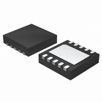
LT1913EDD#PBF Linear Technology, LT1913EDD#PBF Datasheet - Page 11

LT1913EDD#PBF
Manufacturer Part Number
LT1913EDD#PBF
Description
IC REG STEP DOWN 3.5A 10-DFN
Manufacturer
Linear Technology
Type
Step-Down (Buck)r
Datasheet
1.LT1913EDDPBF.pdf
(24 pages)
Specifications of LT1913EDD#PBF
Internal Switch(s)
Yes
Synchronous Rectifier
No
Number Of Outputs
1
Voltage - Output
0.79 ~ 25 V
Current - Output
3.5A
Frequency - Switching
200kHz ~ 2.4MHz
Voltage - Input
3.6 ~ 25 V
Operating Temperature
-40°C ~ 125°C
Mounting Type
Surface Mount
Package / Case
10-DFN
Primary Input Voltage
25V
No. Of Outputs
1
Output Voltage
25V
Output Current
3.5A
No. Of Pins
10
Operating Temperature Range
-40°C To +125°C
Msl
MSL 1 - Unlimited
Rohs Compliant
Yes
Lead Free Status / RoHS Status
Lead free / RoHS Compliant
Power - Output
-
Available stocks
Company
Part Number
Manufacturer
Quantity
Price
APPLICATIONS INFORMATION
operating input voltage. Conversely, a lower switching
frequency will be necessary to achieve safe operation at
high input voltages.
If the output is in regulation and no short-circuit, start-
up, or overload events are expected, then input voltage
transients of up to 25V are acceptable regardless of the
switching frequency. In this mode, the LT1913 may enter
pulse skipping operation where some switching pulses
are skipped to maintain output regulation. In this mode
the output voltage ripple and inductor current ripple will
be higher than in normal operation.
The minimum input voltage is determined by either the
LT1913’s minimum operating voltage of ~3.6V or by its
maximum duty cycle (see equation in previous section).
The minimum input voltage due to duty cycle is:
where V
is the minimum switch off time (150ns). Note that higher
switching frequency will increase the minimum input
voltage. If a lower dropout voltage is desired, a lower
switching frequency should be used.
Inductor Selection
For a given input and output voltage, the inductor value
and switching frequency will determine the ripple current.
The ripple current ΔI
and decreases with higher inductance and faster switch-
ing frequency. A reasonable starting point for selecting
the ripple current is:
where I
guarantee suffi cient output current, peak inductor current
must be lower than the LT1913’s switch current limit (I
The peak inductor current is:
where I
the maximum output load current, and ΔI
ΔI
I
V
L(PEAK)
IN MIN
L
(
= 0.4(I
OUT(MAX)
L(PEAK)
IN(MIN)
) =
= I
OUT(MAX)
OUT(MAX)
1– f
is the minimum input voltage, and t
is the peak inductor current, I
V
is the maximum output load current. To
SW
OUT
t
L
OFF MIN
+ V
)
increases with higher V
+ ΔI
(
D
L
/2
)
– V
D
+ V
SW
L
is the inductor
OUT(MAX)
IN
OFF(MIN)
or V
LIM
OUT
is
).
ripple current. The LT1913’s switch current limit (I
5.5A at low duty cycles and decreases linearly to 4.5A at
DC = 0.8. The maximum output current is a function of
the inductor ripple current:
Be sure to pick an inductor ripple current that provides
suffi cient maximum output current (I
The largest inductor ripple current occurs at the highest
V
specifi ed maximum, the inductor value should be chosen
according to the following equation:
where V
V
voltage, f
L is in the inductor value.
The inductor’s RMS current rating must be greater than the
maximum load current and its saturation current should be
about 30% higher. To keep the effi ciency high, the series
resistance (DCR) should be less than 0.05 , and the core
material should be intended for high frequency applications.
Table 1 lists several vendors and suitable types.
Table 1. Inductor Vendors
Of course, such a simple design guide will not always re-
sult in the optimum inductor for your application. A larger
value inductor provides a slightly higher maximum load
current and will reduce the output voltage ripple. If your
VENDOR
Murata
TDK
Toko
Sumida
NEC
IN
IN(MAX)
I
L =
. To guarantee that the ripple current stays below the
OUT(MAX)
D
V
is the maximum input voltage, V
SW
OUT
f
is the voltage drop of the catch diode (~0.4V),
SW
URL
www.murata.com
www.componenttdk.com
www.toko.com
www.sumida.com
www.nec.com
= I
is the switching frequency (set by RT), and
+ V
I
LIM
L
D
– ΔI
1–
L
/2
V
V
OUT
IN(MAX)
+ V
PART SERIES
LQH55D
SLF10145
D75C
D75F
CDRH74
CR75
CDRH8D43
MPLC073
MPBI0755
D
OUT(MAX)
OUT
LT1913
is the output
).
TYPE
Open
Shielded
Shielded
Open
Shielded
Open
Shielded
Shielded
Shielded
11
LIM
1913f
) is


