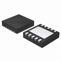
LT1913EDD#PBF Linear Technology, LT1913EDD#PBF Datasheet - Page 14

LT1913EDD#PBF
Manufacturer Part Number
LT1913EDD#PBF
Description
IC REG STEP DOWN 3.5A 10-DFN
Manufacturer
Linear Technology
Type
Step-Down (Buck)r
Datasheet
1.LT1913EDDPBF.pdf
(24 pages)
Specifications of LT1913EDD#PBF
Internal Switch(s)
Yes
Synchronous Rectifier
No
Number Of Outputs
1
Voltage - Output
0.79 ~ 25 V
Current - Output
3.5A
Frequency - Switching
200kHz ~ 2.4MHz
Voltage - Input
3.6 ~ 25 V
Operating Temperature
-40°C ~ 125°C
Mounting Type
Surface Mount
Package / Case
10-DFN
Primary Input Voltage
25V
No. Of Outputs
1
Output Voltage
25V
Output Current
3.5A
No. Of Pins
10
Operating Temperature Range
-40°C To +125°C
Msl
MSL 1 - Unlimited
Rohs Compliant
Yes
Lead Free Status / RoHS Status
Lead free / RoHS Compliant
Power - Output
-
Available stocks
Company
Part Number
Manufacturer
Quantity
Price
APPLICATIONS INFORMATION
LT1913
V
and a resistor (R
tion, there may be lower value capacitor in parallel. This
capacitor (C
is used to fi lter noise at the switching frequency, and is
required only if a phase-lead capacitor is used or if the
output capacitor has high ESR.
Loop compensation determines the stability and transient
performance. Designing the compensation network is a bit
complicated and the best values depend on the application
and in particular the type of output capacitor. A practical
approach is to start with one of the circuits in this data
sheet that is similar to your application and tune the com-
pensation network to optimize the performance. Stability
should then be checked across all operating conditions,
including load current, input voltage and temperature. The
LT1375 data sheet contains a more thorough discussion of
loop compensation and describes how to test the stabil-
ity using a transient load. Figure 2 shows an equivalent
circuit for the LT1913 control loop. The error amplifi er is a
transconductance amplifi er with fi nite output impedance.
The power section, consisting of the modulator, power
switch and inductor, is modeled as a transconductance
amplifi er generating an output current proportional to
the voltage at the V
integrates this current, and that the capacitor on the V
(C
in two poles in the loop. In most cases a zero is required
and comes from either the output capacitor ESR or from
a resistor R
well as long as the value of the inductor is not too high
and the loop crossover frequency is much lower than the
switching frequency. A phase lead capacitor (C
the feedback divider may improve the transient response.
Figure 3 shows the transient response when the load cur-
rent is stepped from 1A to 3A and back to 1A.
14
C
C
pin, as shown in Figure 2. Generally a capacitor (C
) integrates the error amplifi er output current, resulting
C
F
) is not part of the loop compensation but
in series with C
C
) in series to ground are used. In addi-
C
pin. Note that the output capacitor
C
. This simple model works
PL
) across
C
pin
C
)
BOOST and BIAS Pin Considerations
Capacitor C3 and the internal boost Schottky diode (see
the Block Diagram) are used to generate a boost volt-
age that is higher than the input voltage. In most cases
a 0.47μF capacitor will work well. Figure 2 shows three
ways to arrange the boost circuit. The BOOST pin must be
Figure 3. Transient Load Response of the LT1913 Front Page
Application as the Load Current is Stepped from 1A to 3A.
V
LT1913
OUT
CURRENT MODE
POWER STAGE
g
m
100mV/DIV
C
= 5V
F
= 5.3mho
1A/DIV
V
R
V
C
C
OUT
3M
C
C
I
Figure 2. Model for Loop Response
L
525μmho
g
AMPLIFIER
m
ERROR
=
–
+
GND
0.8V
10μs/DIV
SW
FB
R1
R2
TANTALUM
POLYMER
C
PL
ESR
C1
OR
1913 F03
+
1913 F02
OUTPUT
C1
CERAMIC
1913f


