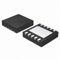
LT1913EDD#PBF Linear Technology, LT1913EDD#PBF Datasheet - Page 9

LT1913EDD#PBF
Manufacturer Part Number
LT1913EDD#PBF
Description
IC REG STEP DOWN 3.5A 10-DFN
Manufacturer
Linear Technology
Type
Step-Down (Buck)r
Datasheet
1.LT1913EDDPBF.pdf
(24 pages)
Specifications of LT1913EDD#PBF
Internal Switch(s)
Yes
Synchronous Rectifier
No
Number Of Outputs
1
Voltage - Output
0.79 ~ 25 V
Current - Output
3.5A
Frequency - Switching
200kHz ~ 2.4MHz
Voltage - Input
3.6 ~ 25 V
Operating Temperature
-40°C ~ 125°C
Mounting Type
Surface Mount
Package / Case
10-DFN
Primary Input Voltage
25V
No. Of Outputs
1
Output Voltage
25V
Output Current
3.5A
No. Of Pins
10
Operating Temperature Range
-40°C To +125°C
Msl
MSL 1 - Unlimited
Rohs Compliant
Yes
Lead Free Status / RoHS Status
Lead free / RoHS Compliant
Power - Output
-
Available stocks
Company
Part Number
Manufacturer
Quantity
Price
OPERATION
The LT1913 is a constant frequency, current mode step-
down regulator. An oscillator, with frequency set by RT,
enables an RS fl ip-fl op, turning on the internal power
switch. An amplifi er and comparator monitor the current
fl owing between the V
off when this current reaches a level determined by the
voltage at V
voltage through an external resistor divider tied to the FB
pin and servos the V
increases, more current is delivered to the output; if it
decreases, less current is delivered. An active clamp on the
V
the voltage on the RUN/SS pin; soft-start is implemented
by generating a voltage ramp at the RUN/SS pin using an
external resistor and capacitor.
An internal regulator provides power to the control circuitry.
The bias regulator normally draws power from the V
but if the BD pin is connected to an external voltage higher
than 3V bias power will be drawn from the external source
(typically the regulated output voltage). This improves
C
pin provides current limit. The V
C
. An error amplifi er measures the output
C
IN
pin. If the error amplifi er’s output
and SW pins, turning the switch
C
pin is also clamped to
IN
pin,
effi ciency. The RUN/SS pin is used to place the LT1913
in shutdown, disconnecting the output and reducing the
input current to less than 0.5μA.
The switch driver operates from either the input or from
the BOOST pin. An external capacitor and diode are used
to generate a voltage at the BOOST pin that is higher than
the input supply. This allows the driver to fully saturate
the internal bipolar NPN power switch for effi cient opera-
tion.
The oscillator reduces the LT1913’s operating frequency
when the voltage at the FB pin is low. This frequency
foldback helps to control the output current during startup
and overload.
The LT1913 contains a power good comparator which trips
when the FB pin is at 91% of its regulated value. The PG
output is an open-collector transistor that is off when the
output is in regulation, allowing an external resistor to pull
the PG pin high. Power good is valid when the LT1913 is
enabled and V
IN
is above 3.6V.
LT1913
9
1913f


