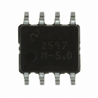
LM2597M-5.0/NOPB National Semiconductor, LM2597M-5.0/NOPB Datasheet - Page 22

LM2597M-5.0/NOPB
Manufacturer Part Number
LM2597M-5.0/NOPB
Description
IC REG SIMPLE SWITCHER 8-SOIC
Manufacturer
National Semiconductor
Series
SIMPLE SWITCHER®r
Type
Step-Down (Buck)r
Datasheet
1.LM2597M-3.3NOPB.pdf
(34 pages)
Specifications of LM2597M-5.0/NOPB
Internal Switch(s)
Yes
Synchronous Rectifier
No
Number Of Outputs
1
Voltage - Output
5V
Current - Output
500mA
Frequency - Switching
150kHz
Voltage - Input
4.5 ~ 40 V
Operating Temperature
-40°C ~ 125°C
Mounting Type
Surface Mount
Package / Case
8-SOIC (3.9mm Width)
Primary Input Voltage
12V
No. Of Outputs
1
Output Voltage
5V
Output Current
500mA
No. Of Pins
8
Operating Temperature Range
-40°C To +125°C
Supply Voltage Range
4.5V To 40V
Filter Terminals
SMD
Rohs Compliant
Yes
Input Voltage Primary Max
40V
Lead Free Status / RoHS Status
Lead free / RoHS Compliant
Power - Output
-
Other names
*LM2597M-5.0
*LM2597M-5.0/NOPB
LM2597M-5.0
*LM2597M-5.0/NOPB
LM2597M-5.0
Available stocks
Company
Part Number
Manufacturer
Quantity
Price
Part Number:
LM2597M-5.0/NOPB
Manufacturer:
TI/德州仪器
Quantity:
20 000
www.national.com
Application Information
DELAY CAPACITOR
C
upper curve in Figure 13 , and also refer to timing diagrams in
Figure 14 . A capacitor on this pin provides a time delay
between the time the regulated output voltage (when it is
increasing in value) reaches 95% of the nominal output
voltage, and the time the error flag output goes high. A 3 µA
constant current from the delay pin charges the delay ca-
pacitor resulting in a voltage ramp. When this voltage
reaches a threshold of approximately 1.3V, the open collec-
tor error flag output (or power OK) goes high. This signal can
be used to indicate that the regulated output has reached the
correct voltage and has stabilized.
If, for any reason, the regulated output voltage drops by 5%
or more, the error output flag (Pin 1) immediately goes low
(internal transistor turns on). The delay capacitor provides
very little delay if the regulated output is dropping out of
regulation. The delay time for an output that is decreasing is
approximately a 1000 times less than the delay for the rising
output. For a 0.1 µF delay capacitor, the delay time would be
DELAY
— Provides delay for the error flag output. See the
FIGURE 15. External 3.7V Soft-Start Clamp
FIGURE 14. Timing Diagram for 5V Output
(Continued)
22
approximately 50 ms when the output is rising and passes
through the 95% threshold, but the delay for the output
dropping would only be approximately 50 µs.
R
lector of a NPN transistor, with the emitter internally
grounded. To use the error flag, a pullup resistor to a positive
voltage is needed. The error flag transistor is rated up to a
maximum of 45V and can sink approximately 3 mA. If the
error flag is not used, it can be left open.
INPUT CAPACITOR
C
needed between the input pin and ground pin. It must be
located near the regulator using short leads. This capacitor
prevents large voltage transients from appearing at the in-
put, and provides the instantaneous current needed each
time the switch turns on.
The important parameters for the Input capacitor are the
voltage rating and the RMS current rating. Because of the
relatively high RMS currents flowing in a buck regulator’s
input capacitor, this capacitor should be chosen for its RMS
Pull Up
IN
— A low ESR aluminum or tantalum bypass capacitor is
— The error flag output, (or power OK) is the col-
DS012440-75
DS012440-34


