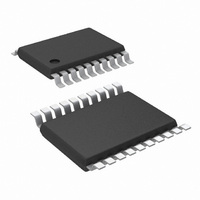
LM20323MH/NOPB National Semiconductor, LM20323MH/NOPB Datasheet - Page 2

LM20323MH/NOPB
Manufacturer Part Number
LM20323MH/NOPB
Description
IC REG SYNC BUCK 3A ADJ 20TSSOP
Manufacturer
National Semiconductor
Series
PowerWise®r
Type
Step-Down (Buck)r
Datasheet
1.LM20323MHNOPB.pdf
(20 pages)
Specifications of LM20323MH/NOPB
Internal Switch(s)
Yes
Synchronous Rectifier
Yes
Number Of Outputs
1
Voltage - Output
0.8 ~ 32 V
Current - Output
3A
Frequency - Switching
520kHz
Voltage - Input
4.5 ~ 36 V
Operating Temperature
-40°C ~ 125°C
Mounting Type
Surface Mount
Package / Case
20-TSSOP Exposed Pad, 20-eTSSOP, 20-HTSSOP
For Use With
LM20323EVAL - EVALUATION BOARD FOR THE LM20323
Lead Free Status / RoHS Status
Lead free / RoHS Compliant
Power - Output
-
Other names
LM20323MH
www.national.com
5,6,15,16
7,8,13,14
9,10,11
Pin(s)
Connection Diagram
Ordering Information
Pin Descriptions
Order Number
EP
12
17
18
19
20
LM20323MHE
LM20323MHX
1
2
3
4
LM20323MH
Exposed
PGOOD
SS/TRK
COMP
AGND
BOOT
Name
GND
VCC
Pad
VIN
SW
NC
FB
EN
Description
Soft-Start or Tracking control input
Feedback input to the error amplifier
from the regulated output
Power good output signal
Output of the internal error amplifier and
input to the Pulse Width Modulator
Input supply voltage
Switch pin
Ground
Analog ground
Boost input for bootstrap capacitor
Output of the high voltage linear
regulator. The VCC voltage is regulated
to approximately 5.5V.
Enable or UVLO input
No Connection
Exposed pad
Package Type
eTSSOP-20
NSC Package Drawing
eTSSOP-20 Package
MXA20A
Top View
Application Information
An internal 4.5 µA current source charges an external capacitor to set
the soft-start rate. The PWM can track to an external voltage ramp with
a low impedance source. If left open, an internal 1 ms SS ramp is
activated.
This pin is connected to the inverting input of the internal
transconductance error amplifier. An 800 mV reference is internally
connected to the non-inverting input of the error amplifier.
Open drain output indicating the output voltage is regulating within
tolerance. A pull-up resistor of 10 kΩ to 100 kΩ is recommended if this
function is used.
The loop compensation network should be connected between the
COMP pin and the AGND pin.
Nominal operating range: 4.5V to 36V.
The drain terminal of the internal Synchronous Rectifier power
NMOSFET and the source terminal of the internal Control power
NMOSFET.
Internal reference for the power MOSFETs.
Internal reference for the regulator control functions.
An internal diode from VCC to BOOT charges an external capacitor
required from SW to BOOT to power the Control MOSFET gate driver.
VCC tracks VIN up to about 7.2V. Above VIN = 7.2V, VCC is regulated
to approximately 5.5 Volts. A 0.1 µF to 1 µF ceramic decoupling
capacitor is required. The VCC pin is an output only.
An external voltage divider can be used to set the line undervoltage
lockout threshold. If the EN pin is left unconnected, a 2 µA pull-up
current source pulls the EN pin high to enable the regulator.
Recommend connecting this pin to GND.
Exposed metal pad on the underside of the package with a weak
electrical connection to GND. Connect this pad to the PC board ground
plane in order to improve heat dissipation.
2
Package Marking
30051502
20323MH
2500 Units per Tape and Reel
250 Units per Tape and Reel
73 Units per Rail
Supplied As


