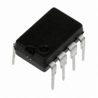
LM2578AN/NOPB National Semiconductor, LM2578AN/NOPB Datasheet - Page 10

LM2578AN/NOPB
Manufacturer Part Number
LM2578AN/NOPB
Description
IC REG SIMPLE SWITCHER 8-DIP
Manufacturer
National Semiconductor
Type
Step-Down (Buck), Step-Up (Boost), Inverting, Flybackr
Datasheet
1.LM3578AMNOPB.pdf
(20 pages)
Specifications of LM2578AN/NOPB
Internal Switch(s)
Yes
Synchronous Rectifier
No
Number Of Outputs
1
Current - Output
750mA
Frequency - Switching
20kHz
Voltage - Input
2 ~ 40 V
Operating Temperature
-40°C ~ 85°C
Mounting Type
Through Hole
Package / Case
8-DIP (0.300", 7.62mm)
No. Of Outputs
1
Output Voltage
1V
Output Current
750mA
No. Of Pins
8
Operating Temperature Range
-40°C To +85°C
Msl
MSL 1 - Unlimited
Input Voltage
40V
Input Voltage Primary Max
40V
Rohs Compliant
Yes
Primary Input Voltage
40V
Lead Free Status / RoHS Status
Lead free / RoHS Compliant
Voltage - Output
-
Power - Output
-
Other names
*LM2578AN
*LM2578AN/NOPB
LM2578AN
*LM2578AN/NOPB
LM2578AN
www.national.com
Applications Information
DUTY CYCLE ADJUSTMENT
When manual or mechanical selection of the output transis-
tor’s duty cycle is needed, the cirucit shown below may be
used. The output will turn on with the beginning of each
oscillator cycle and turn off when the current sunk by R2 and
R3 from the non-inverting terminal becomes greater than the
current sunk from the inverting terminal.
With the resistor values as shown, R3 can be used to adjust
the duty cycle from 0% to 90%.
When the sum of R2 and R3 is twice the value of R1, the
duty cycle will be about 50%. C1 may be a large electrolytic
capacitor to lower the oscillator frequency below 1 Hz.
REMOTE SHUTDOWN
The LM2578A may be remotely shutdown by sinking a
greater current from the non-inverting input than from the
inverting input. This may be accomplished by selecting re-
sistor R3 to be approximately one-half the value of R1 and
R2 in parallel.
FIGURE 9. Maximum Duty Cycle Limiting
FIGURE 10. Duty Cycle Adjustment
00871121
(Continued)
00871123
10
EMITTER OUTPUT
When the LM2578A output transistor is in the OFF state, if
the Emitter output swings below the ground pin voltage, the
output transistor will turn ON because its base is clamped
near ground. The Collector Current with Emitter Output Be-
low Ground curve shows the amount of Collector current
drawn in this mode, vs temperature and Emitter voltage.
When the Collector-Emitter voltage is high, this current will
cause high power dissipation in the output transistor and
should be avoided.
This situation can occur in the high-current high-voltage
buck application if the Emitter output is used and the catch
diode’s forward voltage drop is greater than 0.6V. A fast-
recovery diode can be added in series with the Emitter
output to counter the forward voltage drop of the catch diode
(see Figure 2). For better efficiency of a high output current
buck regulator, an external PNP transistor should be used as
shown in Figure 16.
SYNCHRONIZING DEVICES
When several devices are to be operated at once, their
oscillators may be synchronized by the application of an
external signal. This drive signal should be a pulse waveform
with a minimum pulse width of 2 µs. and an amplitude from
Improperly Turning ON due to D2’s Forward Voltage
FIGURE 12. D1 Prevents Output Transistor from
FIGURE 11. Shutdown Occurs when V
L
is High
00871130
00871124


