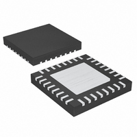
MAX8566ETJ+ Maxim Integrated Products, MAX8566ETJ+ Datasheet

MAX8566ETJ+
Specifications of MAX8566ETJ+
Related parts for MAX8566ETJ+
MAX8566ETJ+ Summary of contents
Page 1
... Pin Configuration appears at end of data sheet. Features ) IN Ordering Information TEMP RANGE PIN-PACKAGE -40°C to +85°C 32 TQFN-EP* Typical Operating Circuit INPUT 2.25V TO 3.6V REFIN PGND SS PGND EN PGND SYNC PGND MAX8566ETJ+ FREQ STEP-DOWN REGULATOR LX TQFN 5mm x 5mm L1 SYNCOUT LX OUTPUT 330nH/10A UP TO 10A GND 22µF 6.3V COMPENSATION 1 ...
Page 2
High-Efficiency, 10A, PWM Internal-Switch Step-Down Regulator ABSOLUTE MAXIMUM RATINGS EN/SS, EN, IN, SYNC LSS, PWRGD to GND ..........-0.3V to +4V (4.5V nonswitching) SYNCOUT, SS, COMP, FB, REFIN, FREQ to GND .........................................-0. Current (Note 1) ...
Page 3
Internal-Switch Step-Down Regulator ELECTRICAL CHARACTERISTICS (continued 3.3V 0.5V PARAMETER FB Input Bias Current V FB REFIN Input Bias Current V REFIN V DD REFIN Common-Mode Range V ...
Page 4
High-Efficiency, 10A, PWM Internal-Switch Step-Down Regulator ELECTRICAL CHARACTERISTICS (continued 3.3V 0.5V SYNC PARAMETER SYNC Capture Range V DD Pulse Width V DD Input Threshold V DD Input ...
Page 5
Internal-Switch Step-Down Regulator ELECTRICAL CHARACTERISTICS ( 3.3V 0.5V PARAMETER IN and V Voltage Range DD LSS Voltage Range IN Supply Current Quiescent current Supply ...
Page 6
High-Efficiency, 10A, PWM Internal-Switch Step-Down Regulator ELECTRICAL CHARACTERISTICS (continued 3.3V 0.5V SYNC PARAMETER Switching Frequency V = 2.5V or 3.3V IN Minimum Off-Time V = 2.5V or ...
Page 7
Internal-Switch Step-Down Regulator ELECTRICAL CHARACTERISTICS (continued 3.3V 0.5V PARAMETER SYNCOUT Frequency Range V DD Phase Shift from SYNC or Frequency = 1MHz Internal Oscillator I SYNCOUT Output ...
Page 8
High-Efficiency, 10A, PWM Internal-Switch Step-Down Regulator (Typical values are 3.3V REFERENCE VOLTAGE vs. TEMPERATURE 0.65 0.64 0.63 0.62 0.61 0.60 0.59 0.58 0.57 0.56 0.55 - 120 TEMPERATURE (°C) ...
Page 9
Internal-Switch Step-Down Regulator (Typical values are 3.3V GAIN/PHASE OF THE VOLTAGE LOOP 0dB GAIN (10dB/div) 0° PHASE (45°/div FREQUENCY (kHz) FULL-LOAD SWITCHING WAVEFORMS 12A I L (2A/div) 10A 0A t ...
Page 10
High-Efficiency, 10A, PWM Internal-Switch Step-Down Regulator (Typical values are 3.3V SOFT-START WITH REFIN 6. (5A/div 0.6V REFIN (500mV/div) 0V 1.8V V OUT (1V/div 400µs/div SOFT-START ...
Page 11
Internal-Switch Step-Down Regulator PIN NAME Monotonic Startup Enable/Disable. Connect MODE to GND or to the center tap of an external 1 MODE resistor-divider to enable/disable monotonic startup mode. Error-Amplifier Output. Connect the necessary compensation network from COMP to FB. COMP ...
Page 12
High-Efficiency, 10A, PWM Internal-Switch Step-Down Regulator SHUTDOWN EN CONTROL BIAS GENERATOR VOLTAGE REFERENCE SS SOFT-START REFIN FB COMP COMP LOW DETECTOR MAX8566 Figure 1. Functional Diagram 12 ______________________________________________________________________________________ V DD UVLO CIRCUITRY CURRENT-LIMIT COMPARATOR ILIM THRESHOLD CONTROL ...
Page 13
Internal-Switch Step-Down Regulator Detailed Description The MAX8566 high-efficiency, voltage-mode switching regulator is capable of delivering up to 10A of output current. The MAX8566 provides output voltages from 0.6V to (0. from 2.3V to 3.6V input supplies, IN ...
Page 14
High-Efficiency, 10A, PWM Internal-Switch Step-Down Regulator R1 REFIN R2 C MAX8566 Figure 2. Soft-Start Implementation with External Reference Undervoltage Lockout (UVLO) The UVLO circuitry inhibits switching when V below 2V. Once V rises above 2V, UVLO clears and DD the ...
Page 15
Internal-Switch Step-Down Regulator square wave at the desired synchronization frequency. A rising edge on SYNC triggers the internal SYNC cir- cuitry. The frequency of the input into SYNC must be higher than the internal oscillator frequency set ...
Page 16
High-Efficiency, 10A, PWM Internal-Switch Step-Down Regulator The peak inductor current (I ) is: P − IN OUT = × I − × Use these equations for initial capacitor selection. Determine final values ...
Page 17
Internal-Switch Step-Down Regulator L LX MAX8566 FB R1 COMP Figure 4. Type 3 Compensation Network determined by the frequencies of the double pole and ESR zero of the power transfer function also a func- tion of the desired ...
Page 18
High-Efficiency, 10A, PWM Internal-Switch Step-Down Regulator GAIN (dB) POWER-STAGE TRANSFER FUNCTION Figure 5. Transfer Function for Type 3 Compensation 2) Connect input and output capacitors to the power ground plane; connect all other capacitors to the sig- nal ground plane. ...
Page 19
Internal-Switch Step-Down Regulator Pin Configuration TOP VIEW REFIN SYNC 28 MAX8566 FREQ 29 30 SYNCOUT GND THIN QFN *CONNECT ...
Page 20
... Maxim cannot assume responsibility for use of any circuitry other than circuitry entirely embodied in a Maxim product. No circuit patent licenses are implied. Maxim reserves the right to change the circuitry and specifications without notice at any time. 20 ____________________Maxim Integrated Products, 120 San Gabriel Drive, Sunnyvale, CA 94086 408-737-7600 © 2011 Maxim Integrated Products ...


