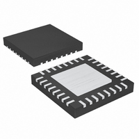
MAX8566ETJ+ Maxim Integrated Products, MAX8566ETJ+ Datasheet - Page 15

MAX8566ETJ+
Manufacturer Part Number
MAX8566ETJ+
Description
IC REG STP DWN 10A 32-TQFN
Manufacturer
Maxim Integrated Products
Type
Step-Down (Buck)r
Datasheet
1.MAX8566ETJ.pdf
(20 pages)
Specifications of MAX8566ETJ+
Internal Switch(s)
Yes
Synchronous Rectifier
No
Number Of Outputs
1
Voltage - Output
0.6 ~ 3.1 V
Current - Output
10A
Frequency - Switching
250kHz ~ 4.2MHz
Voltage - Input
2.3 ~ 3.6 V
Operating Temperature
-40°C ~ 85°C
Mounting Type
Surface Mount
Package / Case
32-TQFN Exposed Pad
Power - Output
2.67W
Output Voltage
0.5 V
Input Voltage
2.3 V to 3.6 V
Switching Frequency
2 MHz
Operating Temperature Range
- 40 C to + 85 C
Mounting Style
SMD/SMT
Duty Cycle (max)
95 %
Lead Free Status / RoHS Status
Lead free / RoHS Compliant
square wave at the desired synchronization frequency.
A rising edge on SYNC triggers the internal SYNC cir-
cuitry. The frequency of the input into SYNC must be
higher than the internal oscillator frequency set by
R
tion and operate on the internal oscillator.
The MAX8566 has a SYNCOUT output that generates a
clock signal that is 180° out-of-phase with its internal
oscillator, or the signal applied to SYNC. This allows for
another regulator to be synchronized 180° out-of-phase
to reduce the input ripple current.
PWRGD is an open-drain output that goes high imped-
ance once the soft-start ramp has concluded, provided
V
below 0.54V for at least 50µs. PWRGD is low during
shutdown.
The MAX8566 provides an external input for the low-
side MOSFET driver supply (LSS). This allows for high-
er gate-drive voltages to maximize converter efficiency
at low input voltages.
Drive EN to GND to shut down the IC and reduce qui-
escent current to 4µA. During shutdown, the output is
high impedance. Drive EN high to enable the
MAX8566.
Thermal-overload protection limits total power dissipa-
tion in the device. When the junction temperature
exceeds T
device into shutdown, allowing the die to cool. The ther-
mal sensor turns the device on again after the junction
temperature cools by 20°C, causing a pulsed output
during continuous overload conditions. The soft-start
sequence begins after a thermal-shutdown condition.
To decrease the noise effects due to the high switching
frequency and maximize the output accuracy of the
MAX8566, decouple V
V
the capacitor as close to V
FB
DD
FREQ
is above 0.54V. PWRGD pulls low when V
to GND and a 2Ω resistor from V
Low-Side MOSFET Driver Supply (LSS)
. Leave SYNC disconnected to disable the func-
J
= +165°C a thermal sensor forces the
Applications Information
Power-Good Output (PWRGD)
______________________________________________________________________________________
DD
Internal-Switch Step-Down Regulator
DD
with a 4.7µF capacitor from
as possible.
Thermal Protection
Shutdown Mode
V
DD
DD
Decoupling
to V
IN
. Place
FB
High-Efficiency, 10A, PWM
is
Choose an inductor with the following equation:
where LIR is the ratio of the inductor ripple current to
average continuous current at the minimum duty cycle.
Choose the LIR between 20% to 40% for best perfor-
mance and stability.
Use a low-loss inductor with the lowest possible DC
resistance that fits in the allotted dimensions. Powered
iron ferrite core types are often the best choice for per-
formance. With any core material the core must be
large enough not to saturate at the peak inductor cur-
rent (I
The key selection parameters for the output capacitor
are capacitance, ESR, ESL, and voltage rating require-
ments. These affect the overall stability, output ripple
voltage, and transient response of the DC-DC convert-
er. The output ripple occurs due to variations in the
charge stored in the output capacitor, the voltage drop
due to the capacitor’s ESR, and the voltage drop due to
the capacitor’s ESL. Calculate the output voltage ripple
due to the output capacitance, ESR, and ESL as:
where the output ripple due to output capacitance,
ESR, and ESL are:
V
or V
RIPPLE
RIPPLE ESL
PEAK
= V
). Calculate I
I
L
(
PEAK
V
RIPPLE(C)
=
V
V
RIPPLE C
RIPPLE ESL
RIPPLE ESR
)
f
s
=
=
V
×
t
OUT
I I
⎛
⎝ ⎜
Output Capacitor Selection
V
P P
OFF
1
( )
IN
−
(
(
+
PEAK
+ V
×
LIR
=
×
×
2
LIR I
)
)
(
RIPPLE(ESR)
8
ESL whichever is greater
V
=
=
⎞
⎠ ⎟
×
IN
as follows:
I
I
t
×
P P
P P
×
C
ON
,
−
−
I
−
OUT MA
P P
OUT
I
V
OUT MAX
−
OUT
×
×
Inductor Design
E
(
ESL
×
(
S S R
)
f
+ V
s
X X )
)
RIPPLE(ESL)
.
15


