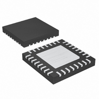
MAX8566ETJ+ Maxim Integrated Products, MAX8566ETJ+ Datasheet - Page 2

MAX8566ETJ+
Manufacturer Part Number
MAX8566ETJ+
Description
IC REG STP DWN 10A 32-TQFN
Manufacturer
Maxim Integrated Products
Type
Step-Down (Buck)r
Datasheet
1.MAX8566ETJ.pdf
(20 pages)
Specifications of MAX8566ETJ+
Internal Switch(s)
Yes
Synchronous Rectifier
No
Number Of Outputs
1
Voltage - Output
0.6 ~ 3.1 V
Current - Output
10A
Frequency - Switching
250kHz ~ 4.2MHz
Voltage - Input
2.3 ~ 3.6 V
Operating Temperature
-40°C ~ 85°C
Mounting Type
Surface Mount
Package / Case
32-TQFN Exposed Pad
Power - Output
2.67W
Output Voltage
0.5 V
Input Voltage
2.3 V to 3.6 V
Switching Frequency
2 MHz
Operating Temperature Range
- 40 C to + 85 C
Mounting Style
SMD/SMT
Duty Cycle (max)
95 %
Lead Free Status / RoHS Status
Lead free / RoHS Compliant
ABSOLUTE MAXIMUM RATINGS
EN/SS, EN, IN, SYNC, V
SYNCOUT, SS, COMP, FB, REFIN,
LX Current (Note 1) .................................................-12A to +12A
BST to LX .................................-0.3V to +4V (4.5V nonswitching)
PGND to GND .......................................................-0.3V to +0.3V
High-Efficiency, 10A, PWM
Internal-Switch Step-Down Regulator
Note 1: LX has internal clamp diodes to PGND and IN. Applications that forward bias these diodes should take care not to exceed
Stresses beyond those listed under “Absolute Maximum Ratings” may cause permanent damage to the device. These are stress ratings only, and functional
operation of the device at these or any other conditions beyond those indicated in the operational sections of the specifications is not implied. Exposure to
absolute maximum rating conditions for extended periods may affect device reliability.
ELECTRICAL CHARACTERISTICS
(V
2
IN/V
IN and V
LSS Voltage Range
IN Supply Current
V
Total Shutdown Current into IN
and V
V
Threshold
BST
Shutdown Supply Current
PWM COMPARATOR
Comparator Propagation Delay
COMP
Clamp Voltage, High
Slew Rate
Shutdown Resistance
ERROR AMPLIFIER
FB Regulation Voltage
Error-Amplifier Common-Mode
Input Range
Error-Amplifier Maximum Output
Current
DD
DD
IN
LSS, PWRGD to GND ..........-0.3V to +4V (4.5V nonswitching)
FREQ to GND .........................................-0.3V to (V
_______________________________________________________________________________________
= V
DD
Supply Current
Undervoltage-Lockout
DD
DD
the IC’s package power-dissipation limits.
DD
PARAMETER
= V
Voltage Range
EN
= 3.3V, V
DD
,
FB
= 0.5V, V
Quiescent current, V
f
Quiescent current, V
f
V
3.6V, V
LX starts/stops switching, 2µs
deglitch
V
3.6V or 0V, V
10mV overdrive
V
From COMP to GND, V
V
V
V
S
S
IN
IN
IN
COMP
DD
DD
= 1MHz, no load
= 1MHz, V
SYNC
= V
= V
= 2.3V to 3.6V, V
= 2.3V to 2.6V
= 2.6V to 3.6V
EN
DD
DD
= 1V to 2V, V
= 0V, T
= 0V
= V
= V
EN
LSS
LSS
BST
= 0V
A
DD
= V
= (V
= 3.6V, V
= 0°C to +85°C, typical values are at T
+ 0.3V)
FB
FB
DD
FB
DD
CONDITIONS
BST
EN
= 0.7V
= 0.7V
= 0.7V
= 2.5V and 3.3V
= 0V
- V
LX
LX
=
) =
Continuous Power Dissipation (T
Operating Temperature Range ...........................-40°C to +85°C
Junction Temperature ......................................................+150°C
Storage Temperature Range .............................-65°C to +150°C
Lead Temperature (soldering, 10s) .................................+300°C
Soldering Temperature (reflow) .......................................+260°C
TQFN (derate 33.3mW/°C above +70°C) ..................2666.7W
T
T
V
V
T
T
A
A
A
A
DD
DD
= 0°C to +85°C
= +25°C
= 0°C to +85°C
= +25°C
rising
falling
A
= +25°C, unless otherwise noted.)
0.594
1.72
1.80
0.75
MIN
2.3
2.3
0.8
0
0
A
= +85°C)
TYP
1.90
0.05
0.7
1.8
2.0
2.0
1.4
0.6
14
16
20
30
3
0.606
V
V
MAX
2.15
1.65
100
3.6
3.6
2.2
2.2
1.7
DD
DD
50
10
4
-
-
UNITS
V/µs
mA
mA
mA
µA
µA
ns
Ω
V
V
V
V
V
V


