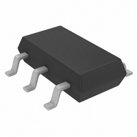
LTC3405AES6#TR Linear Technology, LTC3405AES6#TR Datasheet

LTC3405AES6#TR
Specifications of LTC3405AES6#TR
Available stocks
Related parts for LTC3405AES6#TR
LTC3405AES6#TR Summary of contents
Page 1
... The LTC3405A is available in a low profile (1mm) ThinSOT package. For fixed 1.5V and 1.8V output versions, refer to the LTC3405A-1.5/LTC3405A-1.8 data sheet. , LTC and LT are registered trademarks of Linear Technology Corporation. ThinSOT is a trademark of Linear Technology Corporation. Protected by U.S. Patents, including 6580258, 5481178. V ...
Page 2
... MODE I MODE Leakage Current MODE Burst Mode is a registered trademark of Linear Technology Corporation. Note 1: Absolute Maximum Ratings are those values beyond which the life of a device may be impaired. Note 2: The LTC3405AE is guaranteed to meet performance specifications from 0°C to 70°C. Specifications over the –40°C to 85°C operating temperature range are assured by design, characterization and correlation with statistical process controls ...
Page 3
W U TYPICAL PERFOR A CE CHARACTERISTICS (From Figure1a Except for the Resistive Divider Resistor Values) Efficiency vs Input Voltage 100mA OUT 10mA OUT I = 250mA OUT I = 1mA OUT 80 ...
Page 4
LTC3405A W U TYPICAL PERFOR A CE CHARACTERISTICS (From Figure 1a Except for the Resistive Divider Resistor Values Temperature DS(ON) 1 4. 0.8 0.6 0.4 0.2 ...
Page 5
W U TYPICAL PERFOR A CE CHARACTERISTICS (From Figure 1a Except for the Resistive Divider Resistor Values) Load Step V OUT 100mV/DIV AC COUPLED I L 200mA/DIV I LOAD 200mA/DIV V = 3.6V 40µs/DIV 1.8V OUT I ...
Page 6
LTC3405A CTIO AL DIAGRA MODE 6 SLOPE COMP OSC FREQ SHIFT 0.8V EA – RUN 0.8V REF 1 – OVDET + 0.85V SHUTDOWN U OPERATIO (Refer to Functional Diagram) Main Control ...
Page 7
U OPERATIO (Refer to Functional Diagram) When the converter is in Burst Mode operation, the peak current of the inductor is set to approximately 100mA re- gardless of the output load. Each burst event can last from a few cycles ...
Page 8
LTC3405A U U APPLICATIO S I FOR ATIO The basic LTC3405A application circuit is shown in Fig- ure 1. External component selection is driven by the load requirement and begins with the selection of L followed by C and C ...
Page 9
U U APPLICATIO S I FOR ATIO The selection driven by the required effective OUT series resistance (ESR). Typically, once the ESR require- ment for C has been met, the RMS current rating OUT generally far exceeds ...
Page 10
LTC3405A U U APPLICATIO S I FOR ATIO Although all dissipative elements in the circuit produce losses, two main sources usually account for most of the losses in LTC3405A circuits: V quiescent current and I IN losses. The V quiescent ...
Page 11
U U APPLICATIO S I FOR ATIO The junction temperature given by where T is the ambient temperature example, consider the LTC3405A in dropout at ...
Page 12
LTC3405A U U APPLICATIO S I FOR ATIO 1. The power traces, consisting of the GND trace, the SW trace and the V trace should be kept short, direct and IN wide. 2. Does the V pin connect directly to ...
Page 13
U U APPLICATIO S I FOR ATIO V IN 2. 6.8µ † 22pF C IN LTC3405A 2.2µF 1 CER RUN 6 5 MODE V FB 887k GND *SUMIDA CMD4D11-6R8MC 412k 2 ...
Page 14
LTC3405A U TYPICAL APPLICATIO 2.7V TO 4.2V 100 100 OUTPUT CURRENT (mA) Using All Ceramic ...
Page 15
... MOLD FLASH SHALL NOT EXCEED 0.254mm 6. JEDEC PACKAGE REFERENCE IS MO-193 Information furnished by Linear Technology Corporation is believed to be accurate and reliable. However, no responsibility is assumed for its use. Linear Technology Corporation makes no represen- tation that the interconnection of its circuits as described herein will not infringe on existing patent rights. U ...
Page 16
... IN to 500mA, 1MHz Operation, OUT Pin, Constant Frequency 600mA, REF OUT from 2. 10V 10µ 600mA OUT 10µ 600mA OUT 10µ 600mA OUT LT/TP 0604 1K REV A • PRINTED IN USA © LINEAR TECHNOLOGY CORPORATION 2002 = 3. 3.3V IN 3405afa ...


