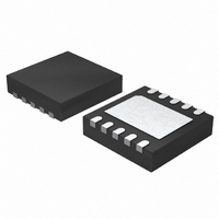
LTC3447EDD Linear Technology, LTC3447EDD Datasheet

LTC3447EDD
Specifications of LTC3447EDD
Available stocks
Related parts for LTC3447EDD
LTC3447EDD Summary of contents
Page 1
... Notebook Computers ■ ■ PDAs and Other Handheld Devices , LTC and LT are registered trademarks of Linear Technology Corporation. Burst Mode is a registered trademark of Linear Technology Corporation. All other trademarks are the property of their respective owners. Protected by U.S. Patents, including 5481178, 6580258, 6304066, 6127815, 6498466, 6611131 ...
Page 2
... I = 100mA, Wafer Level –100mA, Wafer Level 0V 5V RUN SW IN Regulated Feedback Voltage (Note 5) (Note 5) (Note 5) (Note FOR ATIO ORDER PART NUMBER 10 SDA LTC3447EDD 9 V CCD 8 SCL 7 RUN PART MARKING LBKB = 2.96°C/W JC MIN TYP MAX UNITS 0 460 kΩ ● ...
Page 3
ELECTRICAL CHARACTERISTICS temperature range, otherwise specifi cations are at T SYMBOL PARAMETER Interface Timing 2 f Maximum I C Operating Frequency I2C, MAX t Bus Free Time Between Stop and Start Condition (Note 5) BUF t Hold ...
Page 4
LTC3447 W U TYPICAL PERFOR A CE CHARACTERISTICS DAC Nonlinearity 0.5 0.4 0.3 0.2 INL 0.1 0 DNL –0.1 –0.2 –0.3 –0.4 –0 DAC 3447 G04 EffIciency and Power Loss vs Load Current ...
Page 5
W U TYPICAL PERFOR A CE CHARACTERISTICS R vs Supply Voltage DS(ON) 0.60 0.55 0.50 0.45 PFET 0.40 0.35 NFET 0.30 0.25 0.20 2.5 3.5 4.5 SUPPLY VOLTAGE (V) 3447 G10 Feedback Reference vs Supply Voltage 610 605 600 595 ...
Page 6
LTC3447 CTIO S (Pin 1): Output Voltage Sensing Pin. An internal V OUT resistor divider provides the divided down feedback refer- ence for comparison. GND (Pin 2): Ground for all Circuits Excluding the Internal Synchronous ...
Page 7
U OPERATIO BUCK OPERATION V FB PEAK CURRENT LEVEL REF EA V REF RS LATCH S Q OSC R QB LOGIC BURST BUCK REGULATOR Figure 3. LTC3447 Buck Regulator Diagram Main Control Loop The LTC3447 uses current mode step-down architecture ...
Page 8
LTC3447 U OPERATIO the user should calculate the power dissipation when the LTC3447 is used at 100% duty cycle with low input voltage (See Thermal Considerations in the Applications Information section). Low Supply Operation The LTC3447 will operate with input ...
Page 9
U OPERATIO External Start-Up Option The LTC3447 allows for the use of optional external resistors to determine the start-up voltage. Using this option, the start-up voltage can be set to levels inside or outside the DAC output’s operating range. The ...
Page 10
LTC3447 U OPERATIO The START and STOP Commands When the bus is not in use, both SCL and SDA must be high. A bus master signals the beginning of a transmission with a START command by transitioning SDA from high ...
Page 11
U OPERATIO 2 Table Fast-Mode Timing Specifi cations (for Reference Operating Frequency I2C t Bus free time between Stop and Start Condition BUF t Hold Time after (Repeated) Start Condition HD,RSTA t Repeated ...
Page 12
LTC3447 U U APPLICATIO S I FOR ATIO C and C Selection IN OUT In continuous mode, the source current of the top MOSFET is a square wave of duty cycle V OUT voltage transients, a low ESR input capacitor ...
Page 13
U U APPLICATIO S I FOR ATIO loss dominates the effi ciency loss at medium to high load currents typical effi ciency plot, the effi ciency curve at very low load currents can be misleading since the actual ...
Page 14
LTC3447 U U APPLICATIO S I FOR ATIO junction temperature of the part. The temperature rise is given by θ • where P is the power dissipated by the regulator and D θ is ...
Page 15
... DRAWING NOT TO SCALE 3. ALL DIMENSIONS ARE IN MILLIMETERS Information furnished by Linear Technology Corporation is believed to be accurate and reliable. However, no responsibility is assumed for its use. Linear Technology Corporation makes no representation that the interconnection of its circuits as described herein will not infringe on existing patent rights ∆ ...
Page 16
... Dual DC/DC Converter with USB Power Manager and Li-Ion Battery Charger LTC4055 USB Power Manager and Li-Ion Battery Charger LTC4411/LTC4412 PowerPath Controllers in ThinSOT ThinSOT, VLDO and PowerPath are trademarks of Linear Technology Corporation. Linear Technology Corporation 16 1630 McCarthy Blvd., Milpitas, CA 95035-7417 (408) 432-1900 ● ...


