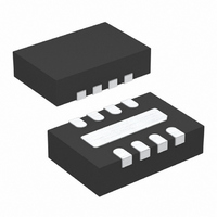
LTC3419EDD-1#TRPBF Linear Technology, LTC3419EDD-1#TRPBF Datasheet

LTC3419EDD-1#TRPBF
Specifications of LTC3419EDD-1#TRPBF
Available stocks
Related parts for LTC3419EDD-1#TRPBF
LTC3419EDD-1#TRPBF Summary of contents
Page 1
... Table 2). , LT, LTC and LTM are registered trademarks of Linear Technology Corporation. Burst Mode is a registered trademark of Linear Technology Corporation. All other trademarks are the property of their respective owners. Protected by U.S. Patents, including 5481178, 6127815, 6304066, 6498466, 6580258, 6611131. ...
Page 2
... PLASTIC DFN = 125°C, θ 40°C/W JMAX JA EXPOSED PAD (PIN 9) IS GND, MUST BE SOLDERED TO PCB ORDER INFORMATION LEAD FREE FINISH TAPE AND REEL LTC3419EDD#PBF LTC3419EDD#TRPBF LTC3419EDD-1#PBF LTC3419EDD-1#TRPBF LTC3419IDD#PBF LTC3419IDD#TRPBF LTC3419IDD-1#PBF LTC3419IDD-1#TRPBF LTC3419EMS#PBF LTC3419EMS#TRPBF LTC3419EMS-1#PBF LTC3419EMS-1#TRPBF LTC3419IMS#PBF LTC3419IMS#TRPBF LTC3419IMS-1#PBF LTC3419IMS-1#TRPBF Consult LTC Marketing for parts specifi ...
Page 3
ELECTRICAL CHARACTERISTICS junction temperature range, otherwise specifi cations are at T SYMBOL PARAMETER V V Operating Voltage Undervoltage Lockout Feedback Pin Input Current FB V Regulated Feedback Voltage (Channel 1) LTC3419E, 0°C < ...
Page 4
LTC3419 TYPICAL PERFORMANCE CHARACTERISTICS Burst Mode Operation SW 2V/DIV V OUT 50mV/DIV AC-COUPLED I L 100mA/DIV 2μs/DIV 1.8V OUT I = 25mA LOAD Reference Voltage vs Temperature 1.5 1.0 0.5 0 –0.5 –1.0 –1.5 ...
Page 5
TYPICAL PERFORMANCE CHARACTERISTICS Effi ciency vs Load Current 100 4.2V OUT 100 OUTPUT ...
Page 6
LTC3419 TYPICAL PERFORMANCE CHARACTERISTICS Load Step V OUT 100mV/DIV AC-COUPLED I L 500mA/DIV I LOAD 500mA/DIV 20μs/DIV 1.8V OUT 600mA LOAD PIN FUNCTIONS (DD/MS) V (Pin 1/Pin 1): Regulator 1 ...
Page 7
FUNCTIONAL DIAGRAM REGULATOR 1 MODE 3 V – FB1 0.6V SOFT-START SHUTDOWN 2 RUN1 0.6V REF OSC 7 RUN2 REGULATOR 2 (IDENTICAL TO REGULATOR FB2 BURST CLAMP SLOPE COMP – SLEEP ...
Page 8
LTC3419 OPERATION The LTC3419 uses a constant-frequency, current mode architecture. The operating frequency is set at 2.25MHz. Both channels share the same clock and run in-phase. The output voltage is set by an external resistor divider returned to the V ...
Page 9
APPLICATIONS INFORMATION A general LTC3419 application circuit is shown in Figure 1. External component selection is driven by the load requirement, and begins with the selection of the inductor L. Once the inductor is chosen, C can be selected. Inductor ...
Page 10
LTC3419 APPLICATIONS INFORMATION deviations do not offer much relief. Note that capacitor manufacturer’s ripple current ratings are often based on only 2000 hours lifetime. This makes it advisable to further derate the capacitor, or choose a capacitor rated at a ...
Page 11
... Effi ciency Considerations The percent effi ciency of a switching regulator is equal to the output power divided by the input power times 100%. Hot Swap is a trademark of Linear Technology Corporation often useful to analyze individual losses to determine what is limiting the effi ciency and which change would produce the most improvement. Percent effi ...
Page 12
LTC3419 APPLICATIONS INFORMATION The R for both the top and bottom MOSFETs can be DS(ON) obtained from the Typical Performance Characteristics 2 curves. Thus, to obtain I R losses losses = I • ...
Page 13
APPLICATIONS INFORMATION 2.5V TO 5.5V V OUT2 BOLD LINES INDICATE HIGH CURRENT PATHS Figure 2. LTC3419 Layout Diagram (See Board Layout Checklist) Design Example As a design example, consider using the LTC3419 in a portable application with a Li-Ion battery. ...
Page 14
LTC3419 APPLICATIONS INFORMATION Using the same analysis for channel 2 (V the results are 1.9μ 59k R4 = 118k C = 22pF F2 Figure 4 shows the complete schematic for this example, along with the effi ...
Page 15
... MOLD FLASH, PROTRUSIONS OR GATE BURRS SHALL NOT EXCEED 0.152mm (.006") PER SIDE Information furnished by Linear Technology Corporation is believed to be accurate and reliable. However, no responsibility is assumed for its use. Linear Technology Corporation makes no representation that the interconnection of its circuits as described herein will not infringe on existing patent rights. ...
Page 16
... Dual 400mA and 800mA I LTC3548-2 2.25MHz, Synchronous Step-Down DC/DC Converters LTC3561 1.25A I , 4MHz, Synchronous OUT Step-Down DC/DC Converter ThinSOT™ trademark of Linear Technology Corporation. Linear Technology Corporation 16 1630 McCarthy Blvd., Milpitas, CA 95035-7417 (408) 432-1900 FAX: (408) 434-0507 ● 2.5V TO 5.5V L1 3.3μH ...


