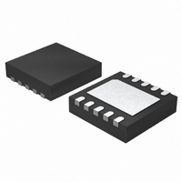
LT3481HDD#TRPBF Linear Technology, LT3481HDD#TRPBF Datasheet - Page 14

LT3481HDD#TRPBF
Manufacturer Part Number
LT3481HDD#TRPBF
Description
IC REG STP DWN ADJ 2A 10-DFN
Manufacturer
Linear Technology
Type
Step-Down (Buck)r
Datasheet
1.LT3481EDDPBF.pdf
(24 pages)
Specifications of LT3481HDD#TRPBF
Internal Switch(s)
Yes
Synchronous Rectifier
No
Number Of Outputs
1
Voltage - Output
1.27 ~ 20 V
Current - Output
2A
Frequency - Switching
300kHz ~ 2.8MHz
Voltage - Input
3.6 ~ 34 V
Operating Temperature
-40°C ~ 150°C
Mounting Type
Surface Mount
Package / Case
10-DFN
Lead Free Status / RoHS Status
Lead free / RoHS Compliant
Power - Output
-
Available stocks
Company
Part Number
Manufacturer
Quantity
Price
APPLICATIONS INFORMATION
LT3481
Burst Mode Operation
To enhance effi ciency at light loads, the LT3481 auto-
matically switches to Burst Mode operation which keeps
the output capacitor charged to the proper voltage while
minimizing the input quiescent current. During Burst Mode
operation, the LT3481 delivers single cycle bursts of current
to the output capacitor followed by sleep periods where
the output power is delivered to the load by the output
capacitor. In addition, V
reduced to typically 20μA and 50μA respectively during
the sleep time. As the load current decreases towards a
no load condition, the percentage of time that the LT3481
operates in sleep mode increases and the average input
current is greatly reduced resulting in higher effi ciency.
See Figure 4.
BOOST and BIAS Pin Considerations
Capacitor C3 and the internal boost Schottky diode (see
the Block Diagram) are used to generate a boost volt-
age that is higher than the input voltage. In most cases
a 0.22μF capacitor will work well. Figure 2 shows three
ways to arrange the boost circuit. The BOOST pin must be
more than 2.3V above the SW pin for best effi ciency. For
outputs of 3V and above, the standard circuit (Figure 5a)
is best. For outputs between 2.8V and 3V, use a 1μF boost
capacitor. A 2.5V output presents a special case because it
is marginally adequate to support the boosted drive stage
while using the internal boost diode. For reliable BOOST pin
operation with 2.5V outputs use a good external Schottky
diode (such as the ON Semi MBR0540), and a 1μF boost
capacitor (see Figure 5b). For lower output voltages the
14
10mV/DIV
0.5A/DIV
5V/DIV
V
V
OUT
SW
I
L
V
I
LOAD
Figure 4. Burst Mode Operation
IN
= 12V; FRONT PAGE APPLICATION
= 10mA
IN
and BIAS quiescent currents are
5μs/DIV
3481 F04
boost diode can be tied to the input (Figure 5c), or to
another supply greater than 2.8V. The circuit in Figure 5a
is more effi cient because the BOOST pin current and BIAS
pin quiescent current comes from a lower voltage source.
You must also be sure that the maximum voltage ratings
of the BOOST and BIAS pins are not exceeded.
The minimum operating voltage of an LT3481 application
is limited by the minimum input voltage (3.6V) and by the
maximum duty cycle as outlined in a previous section. For
proper startup, the minimum input voltage is also limited
by the boost circuit. If the input voltage is ramped slowly,
or the LT3481 is turned on with its RUN/SS pin when the
output is already in regulation, then the boost capacitor
Figure 5. Three Circuits For Generating The Boost Voltage
4.7μF
4.7μF
4.7μF
V
V
V
IN
IN
IN
(5b) For 2.5V < V
V
V
V
IN
IN
IN
(5a) For V
(5c) For V
LT3481
LT3481
LT3481
GND
GND
GND
BD
BD
BD
BOOST
BOOST
BOOST
SW
SW
SW
OUT
OUT
OUT
> 2.8V
< 2.5V
< 2.8V
C3
C3
C3
D2
3481 FO5
V
OUT
V
V
OUT
OUT
3481fc


