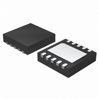
LT3481HDD#TRPBF Linear Technology, LT3481HDD#TRPBF Datasheet - Page 18

LT3481HDD#TRPBF
Manufacturer Part Number
LT3481HDD#TRPBF
Description
IC REG STP DWN ADJ 2A 10-DFN
Manufacturer
Linear Technology
Type
Step-Down (Buck)r
Datasheet
1.LT3481EDDPBF.pdf
(24 pages)
Specifications of LT3481HDD#TRPBF
Internal Switch(s)
Yes
Synchronous Rectifier
No
Number Of Outputs
1
Voltage - Output
1.27 ~ 20 V
Current - Output
2A
Frequency - Switching
300kHz ~ 2.8MHz
Voltage - Input
3.6 ~ 34 V
Operating Temperature
-40°C ~ 150°C
Mounting Type
Surface Mount
Package / Case
10-DFN
Lead Free Status / RoHS Status
Lead free / RoHS Compliant
Power - Output
-
Available stocks
Company
Part Number
Manufacturer
Quantity
Price
APPLICATIONS INFORMATION
LT3481
fi rst plot is the response with a 4.7μF ceramic capacitor
at the input. The input voltage rings as high as 50V and
the input current peaks at 26A. A good solution is shown
in Figure 10b. A 0.7Ω resistor is added in series with the
input to eliminate the voltage overshoot (it also reduces
the peak input current). A 0.1μF capacitor improves high
frequency fi ltering. For high input voltages its impact on
effi ciency is minor, reducing effi ciency by 1.5 percent for
a 5V output at full load operating from 24V.
High Temperature Considerations
The PCB must provide heat sinking to keep the LT3481
cool. The Exposed Pad on the bottom of the package must
be soldered to a ground plane. This ground should be tied
to large copper layers below with thermal vias; these lay-
ers will spread the heat dissipated by the LT3481. Place
additional vias can reduce thermal resistance further. With
these steps, the thermal resistance from die (or junction)
to ambient can be reduced to θ
100LFPM airfl ow, this resistance can fall by another 25%.
Further increases in airfl ow will lead to lower thermal re-
sistance. Because of the large output current capability of
TYPICAL APPLICATIONS
18
6.3V TO 34V
4.7μF
V
IN
JA
= 35°C/W or less. With
D: DIODES INC. DFLS240L
L: TAIYO YUDEN NP06DZB6R8M
330pF
20k
60.4k
ON OFF
5V Step-Down Converter
f = 800kHz
RUN/SS
V
RT
PG
C
V
IN
LT3481
GND
the LT3481, it is possible to dissipate enough heat to raise
the junction temperature beyond the absolute maximum
of 125°C (150°C for the H grade). When operating at high
ambient temperatures, the maximum load current should
be derated as the ambient temperature approaches 125°C
(150°C for the H grade).
Power dissipation within the LT3481 can be estimated
by calculating the total power loss from an effi ciency
measurement and subtracting the catch diode loss. The
die temperature is calculated by multiplying the LT3481
power dissipation by the thermal resistance from junction
to ambient.
Other Linear Technology Publications
Application Notes 19, 35 and 44 contain more detailed
descriptions and design information for buck regulators
and other switching regulators. The LT1376 data sheet
has a more extensive discussion of output ripple, loop
compensation and stability testing. Design Note 100
shows how to generate a bipolar output supply using a
buck regulator.
BD
BOOST
BIAS
SW
FB
200k
0.47μF
D
590k
6.8μH
L
3481 TA02
22μF
V
5V
2A
OUT
3481fc


