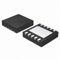
LT3481HDD#TRPBF Linear Technology, LT3481HDD#TRPBF Datasheet - Page 16

LT3481HDD#TRPBF
Manufacturer Part Number
LT3481HDD#TRPBF
Description
IC REG STP DWN ADJ 2A 10-DFN
Manufacturer
Linear Technology
Type
Step-Down (Buck)r
Datasheet
1.LT3481EDDPBF.pdf
(24 pages)
Specifications of LT3481HDD#TRPBF
Internal Switch(s)
Yes
Synchronous Rectifier
No
Number Of Outputs
1
Voltage - Output
1.27 ~ 20 V
Current - Output
2A
Frequency - Switching
300kHz ~ 2.8MHz
Voltage - Input
3.6 ~ 34 V
Operating Temperature
-40°C ~ 150°C
Mounting Type
Surface Mount
Package / Case
10-DFN
Lead Free Status / RoHS Status
Lead free / RoHS Compliant
Power - Output
-
Available stocks
Company
Part Number
Manufacturer
Quantity
Price
APPLICATIONS INFORMATION
LT3481
from 5% up to a maximum value given by the following
equation:
where V
diode forward drop, V
is the switch drop, and f
quency. For example, a 24V input to 5V output at 300kHz
can be synchronized to a square wave with a maximum
duty cycle of 60%. For some applications, such as 12V
to 5V
cycle will be less than 50%. If a low duty cycle clock can-
not be obtained from the system, then a one-shot should
be used between the sync signal and the LT3481. See
Typical Applications.
The value of the coupling capacitor which connects the
clock signal to the RT pin should be chosen based on the
clock signal amplitude. Good starting values for 3.3V and
5V clock signals are 10pF and 5pF, respectively. These
values should be tested and adjusted for each individual
application to assure reliable operation.
Caution should be used when synchronizing more than
50% above the initial switching frequency (as set by
the R
amplitude of the internal slope compensation used to
prevent subharmonic switching is reduced. This type of
subharmonic switching only occurs at input voltages less
than twice output voltage. Higher inductor values will tend
to reduce this problem.
Shorted and Reversed Input Protection
If the inductor is chosen so that it won’t saturate exces-
sively, an LT3481 buck regulator will tolerate a shorted
output. There is another situation to consider in systems
where the output will be held high when the input to the
LT3481 is absent. This may occur in battery charging ap-
plications or in battery backup systems where a battery
or some other supply is diode ORed with the LT3481’s
output. If the V
pin is held high (either by a logic signal or because it is
tied to V
its quiescent current through its SW pin. This is fi ne if
16
DC
T
OUT
SYNC MAX
resistor) because at higher clock frequencies the
OUT
IN
at 350kHz, the maximum allowable sync duty
), then the LT3481’s internal circuitry will pull
(
is the programmed output voltage, V
IN
)
=
pin is allowed to fl oat and the RUN/SS
⎛
⎝ ⎜
1
–
IN
V
is the typical input voltage, V
SW
IN
V
–
OUT
is the desired switching fre-
V
SW
+
V
+
D
V
D
⎞
⎠ ⎟
–
f
SW
• 0 0 0ns
6
D
is the
SW
IN
your system can tolerate a few mA in this state. If you
ground the RUN/SS pin, the SW pin current will drop to
essentially zero. However, if the V
the output is held high, then parasitic diodes inside the
LT3481 can pull large currents from the output through
the SW pin and the V
will run only when the input voltage is present and that
protects against a shorted or reversed input.
PCB Layout
For proper operation and minimum EMI, care must be
taken during printed circuit board layout. Figure 9 shows
the recommended component placement with trace,
ground plane and via locations. Note that large, switched
currents fl ow in the LT3481’s V
diode (D1) and the input capacitor (C1). The loop formed
by these components should be as small as possible. These
components, along with the inductor and output capacitor,
should be placed on the same side of the circuit board,
and their connections should be made on that layer. Place
a local, unbroken ground plane below these components.
The SW and BOOST nodes should be as small as possible.
Finally, keep the FB and V
traces will shield them from the SW and BOOST nodes.
The Exposed Pad on the bottom of the package must be
soldered to ground so that the pad acts as a heat sink. To
keep thermal resistance low, extend the ground plane as
much as possible, and add thermal vias under and near
the LT3481 to additional ground planes within the circuit
board and on the bottom side.
V
IN
Figure 8. Diode D4 Prevents a Shorted Input from
Discharging a Backup Battery Tied to the Output. It Also
Protects the Circuit from a Reversed Input. The LT3481
Runs Only When the Input is Present
MBRS140
D4
V
RUN/SS
V
IN
C
LT3481
GND FB
IN
BOOST
pin. Figure 8 shows a circuit that
C
SW
nodes small so that the ground
IN
IN
and SW pins, the catch
pin is grounded while
3481 F08
V
BACKUP
OUT
3481fc


