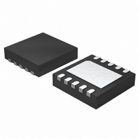
LT3481HDD#TRPBF Linear Technology, LT3481HDD#TRPBF Datasheet - Page 7

LT3481HDD#TRPBF
Manufacturer Part Number
LT3481HDD#TRPBF
Description
IC REG STP DWN ADJ 2A 10-DFN
Manufacturer
Linear Technology
Type
Step-Down (Buck)r
Datasheet
1.LT3481EDDPBF.pdf
(24 pages)
Specifications of LT3481HDD#TRPBF
Internal Switch(s)
Yes
Synchronous Rectifier
No
Number Of Outputs
1
Voltage - Output
1.27 ~ 20 V
Current - Output
2A
Frequency - Switching
300kHz ~ 2.8MHz
Voltage - Input
3.6 ~ 34 V
Operating Temperature
-40°C ~ 150°C
Mounting Type
Surface Mount
Package / Case
10-DFN
Lead Free Status / RoHS Status
Lead free / RoHS Compliant
Power - Output
-
Available stocks
Company
Part Number
Manufacturer
Quantity
Price
PIN FUNCTIONS
BLOCK DIAGRAM
BD (Pin 1): This pin connects to the anode of the boost
Schottky diode.
BOOST (Pin 2): This pin is used to provide a drive
voltage, higher than the input voltage, to the internal bipolar
NPN power switch.
SW (Pin 3): The SW pin is the output of the internal power
switch. Connect this pin to the inductor, catch diode and
boost capacitor.
V
internal regulator and to the internal power switch. This
pin must be locally bypassed.
RUN/SS (Pin 5): The RUN/SS pin is used to put the
LT3481 in shutdown mode. Tie to ground to shut down
the LT3481. Tie to 2.3V or more for normal operation. If
the shutdown feature is not used, tie this pin to the V
pin. RUN/SS also provides a soft-start function; see the
Applications Information section.
IN
(Pin 4): The V
V
IN
R
C1
T
10
4
7
5
6
V
BIAS
RUN/SS
RT
PG
IN
IN
SOFT-START
pin supplies current to the LT3481’s
GND
11
INTERNAL 1.265V REF
+
–
R2
1.12V
8
FB
R1
ERROR AMP
+
–
300kHz TO 2.8MHz
SLOPE COMP
OSCILLATOR
–
+
IN
PG (Pin 6): The PG pin is the open-collector output of an
internal comparator. PG remains low until the FB pin is
within 10% of the fi nal regulation voltage. PG output is
valid when V
BIAS (Pin 7): The BIAS pin supplies the current to the
LT3481’s internal regulator. Tie this pin to the lowest
available voltage source above 3V (typically V
architecture increases effi ciency especially when the input
voltage is much higher than the output.
FB (Pin 8): The LT3481 regulates the FB pin to 1.265V.
Connect the feedback resistor divider tap to this pin.
V
amplifi er. The voltage on this pin controls the peak switch
current. Tie an RC network from this pin to ground to
compensate the control loop.
RT (Pin 10): Oscillator Resistor Input. Connecting a resistor
to ground from this pin sets the switching frequency.
Exposed Pad (Pin 11): Ground. The Exposed Pad must
be soldered to PCB.
C
(Pin 9): The V
Burst Mode
V
R
S
SWITCH
C
LATCH
DETECT
CLAMP
DISABLE
Q
IN
is above 3.5V and RUN/SS is high.
C
pin is the output of the internal error
BOOST
SW
BD
V
C
1
2
3
9
R
C
C
C
C3
D1
L1
C
F
LT3481
C2
OUT
3481 BD
V
OUT
). This
3481fc
7


