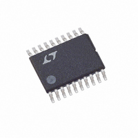
LTC3416EFE Linear Technology, LTC3416EFE Datasheet

LTC3416EFE
Specifications of LTC3416EFE
Available stocks
Related parts for LTC3416EFE
LTC3416EFE Summary of contents
Page 1
... LTC and LT are registered trademarks of Linear Technology Corporation. All other trademarks are the property of their respective owners. OPTI-LOOP is a registered trade- mark of Linear Technology Corporation. Protected by U.S. Patents including 5481178, 6580258, 6304066, 6127815, 6498466, 6611131, 6724174. 22µ ...
Page 2
... Measured in Servo Loop 0.84V ITH (Note 0.7V 1.2V FB ITH RUN R = 294kΩ OSC (Note 300mA –300mA 0V 5.5V RUN ORDER PART NUMBER 20 PGND LTC3416EFE PGOOD PGND = 10°C/W JC http://www.linear.com/leadfree/ MIN TYP MAX UNITS 2.25 5.5 ● 0.784 0.800 0.816 0.2 0.2 0.04 0.2 ...
Page 3
ELECTRICAL CHARACTERISTICS Note 1: Absolute Maximum Ratings are those values beyond which the life of a device may be impaired. The voltage should never exceed 6.0V for any pin. Note 2: The LTC3416E is guaranteed to meet performance specifications from ...
Page 4
LTC3416 W U TYPICAL PERFOR A CE CHARACTERISTICS Frequency vs Temperature 1090 V = 3.3V IN 1070 R = 294k OSC 1050 1030 1010 990 970 950 930 910 –40 – 100 120 60 TEMPERATURE (°C) ...
Page 5
CTIO S PGND (Pins 1, 10, 11, 20): Power Ground. Connect this pin closely to the (–) terminal (Pin 2): Oscillator Resistor Input. Connecting a resistor T to ground from this ...
Page 6
LTC3416 CTIO AL DIAGRA SV SGND VOLTAGE REFERENCE TRACK 3 + – ERROR V AMPLIFIER 0.74V – + – 0.86V RUN/SS 4 RUN PGOOD 17 U OPERATIO Main Control Loop The ...
Page 7
U OPERATIO power MOSFET is turned off and the bottom power MOS- FET is switched on until either the overvoltage condition clears or the bottom MOSFET’s current limit is reached. Voltage Tracking Some microprocessors, ASIC and DSP chips need two ...
Page 8
LTC3416 U U APPLICATIO S I FOR ATIO The basic LTC3416 application circuit is shown in Figure 1a. External component selection is determined by the maxi- mum load current and begins with the selection of the operating frequency and inductor ...
Page 9
U U APPLICATIO S I FOR ATIO prevent large voltage transients from occurring, a low ESR input capacitor sized for the maximum RMS current should be used. The maximum RMS current is given by OUT ...
Page 10
LTC3416 U U APPLICATIO S I FOR ATIO coincidentally or ratiometrically track another output volt- age as shown in Figure 3. If the voltage on the TRACK pin is less than 0.8V, voltage tracking is enabled. During voltage tracking, the ...
Page 11
U U APPLICATIO S I FOR ATIO MASTER V FB LTC3416 SGND SLAVE V TRACK FB LTC3416 SGND Figure 5. Dual Voltage System with Tracking An alternative method of tracking is shown in Figure 5. For the circuit of Figure ...
Page 12
LTC3416 U U APPLICATIO S I FOR ATIO The R for both the top and bottom MOSFETs can DS(ON) be obtained from the Typical Performance Characteris- 2 tics curves. Thus, to obtain I R losses, simply add ...
Page 13
U U APPLICATIO S I FOR ATIO C and C should be sized for a maximum current IN1 IN2 rating of: ⎛ ⎞ ⎜ ⎟ – 1 ...
Page 14
LTC3416 U U APPLICATIO S I FOR ATIO PC Board Layout Checklist When laying out the printed circuit board, the following checklist should be used to ensure proper operation of the LTC3416. Check the following in your layout ...
Page 15
... DIMENSIONS ARE IN 3. DRAWING NOT TO SCALE Information furnished by Linear Technology Corporation is believed to be accurate and reliable. However, no responsibility is assumed for its use. Linear Technology Corporation makes no represen- tation that the interconnection of its circuits as described herein will not infringe on existing patent rights Package 20-Lead Plastic TSSOP (4 ...
Page 16
... IN OUT REF < 1µA, TSSOP16E Package SD : 2.25V to 5V 0.8V 64µA, IN OUT Q : 5.5V to 60V 1.2V, IN OUT < 25µA, TSSOP16E Package SD : 2.5V to 5.5V 2.5V, IN OUT < 1µA, MS Package SD LT 1205 REV A • PRINTED IN USA © LINEAR TECHNOLOGY CORPORATION 2004 10 4316 TA02 3416fa ...


