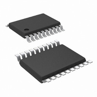
LM5118Q1MHX/NOPB National Semiconductor, LM5118Q1MHX/NOPB Datasheet - Page 22

LM5118Q1MHX/NOPB
Manufacturer Part Number
LM5118Q1MHX/NOPB
Description
IC BUCK BST ADJ 20TSSOP
Manufacturer
National Semiconductor
Series
PowerWise®r
Type
Step-Down (Buck), Step-Up (Boost)r
Datasheet
1.LM5118MHXNOPB.pdf
(26 pages)
Specifications of LM5118Q1MHX/NOPB
Internal Switch(s)
No
Synchronous Rectifier
Yes
Number Of Outputs
1
Voltage - Output
1.23 ~ 70 V
Frequency - Switching
200kHz, 515kHz
Voltage - Input
3 ~ 75 V
Operating Temperature
-40°C ~ 125°C
Mounting Type
Surface Mount
Package / Case
20-TSSOP Exposed Pad, 20-eTSSOP, 20-HTSSOP
Lead Free Status / RoHS Status
Lead free / RoHS Compliant
Current - Output
-
Power - Output
-
Other names
LM5118Q1MHX
Available stocks
Company
Part Number
Manufacturer
Quantity
Price
Company:
Part Number:
LM5118Q1MHX/NOPB
Manufacturer:
BROADCOM
Quantity:
101
Company:
Part Number:
LM5118Q1MHX/NOPB
Manufacturer:
NS/TI
Quantity:
2 600
www.national.com
PCB Layout and Thermal
Considerations
In a buck-boost regulator, there are two loops where currents
are switched very fast. The first loop starts from the input ca-
pacitors, and then to the buck switch, the inductor, the boost
switch then back to the input capacitor. The second loop starts
from the inductor, and then to the output diode, the output
capacitor, the re-circulating diode, and back to the inductor.
Minimizing the PC board area of these two loops reduces the
stray inductance and minimizes noise and the possibility of
erratic operation. A ground plane in the PC board is recom-
mended as a means to connect the input filter capacitors to
the output filter capacitors and the PGND pins of the LM5118.
Connect all of the low current ground connections (C
C
and PGND pins together through topside copper area cover-
ing the entire underside of the device. Place several vias in
this underside copper area to the ground plane of the input
capacitors.
RAMP
) directly to the regulator AGND pin. Connect the AGND
FIGURE 17. VCC Bias with Additional Bias Supply
SS
, R
T
,
22
The highest power dissipating components are the two power
MOSFETs, the re-circulating diode, and the output diode. The
easiest way to determine the power dissipated in the MOS-
FETs is to measure the total conversion losses (P
then subtract the power losses in the Schottky diodes, output
inductor and any snubber resistors. An approximation for the
re-circulating Schottky diode loss is:
P = (1-D) x I
The boost diode loss is
P = I
If a snubber is used, the power loss can be estimated with an
oscilloscope by observation of the resistor voltage drop at
both turn-on and turn-off transitions. The LM5118 package
has an exposed thermal pad to aid power dissipation. Select-
ing diodes with exposed pads will aid the power dissipation of
the diodes as well. When selecting the MOSFETs, pay careful
attention to R
FETs with low gate charge will result in lower switching loss-
es.
OUT
x V
FWD
OUT
DS(ON)
.
x V
at high temperature. Also, selecting MOS-
FWD
.
30058552
IN
- P
OUT
),


