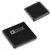
ADMC200AP Analog Devices Inc, ADMC200AP Datasheet - Page 10

ADMC200AP
Manufacturer Part Number
ADMC200AP
Description
IC MOTION CO-PROC 12.5MHZ 68PLCC
Manufacturer
Analog Devices Inc
Datasheet
1.ADMC200AP.pdf
(12 pages)
Specifications of ADMC200AP
Rohs Status
RoHS non-compliant
Applications
*
Mounting Type
Surface Mount
Package / Case
68-PLCC
ADMC200
Name
RHO
PHIP1/VD
PHIP2/VQ
PHIP3
RHOP
PWMTM
PWMCHA
PWMCHB
PWMCHC
PWMDT
PWMPD
SYSCTRL
Figure 11. ADI Digital Signal Processor/Microcomputer
Figure 12. TI Second-Generation Devices TMS320C20/
C25/C25–50
ADSP-2101/
ADSP-2105/
ADSP-2115–20MHz
ADSP-2171–10MHz
ADSP-2181–10MHz
*NOTE:
BY MAPPING THE ADMC200 DATA BUS TO THE TWELVE HIGHEST BITS
OF THE ADSP DATA BUS, FULL-SCALE OUTPUTS FROM THE ADC
CAN BE REPRESENTED BY ± 1.0 IN FIXED POINT ARITHMETIC.
TMS320C20
TMS320C25
TMS320C25-50
A0–A13
D0–D23
A0–A15
D0–D15
CLKOUT1
CLKOUT
STRB
IRQ2
DMS
INTn
R/W
WR
RD
IS
ADDRESS BUS
ADDRESS BUS
DATA BUS
DATA BUS
EN
EN
ADDRESS
ADDRESS
DECODE
DECODE
V
V
DD
DD
A
0
0
0
0
0
0
0
0
1
1
1
1
1
1
1
1
3
RD
CS
IRQ
WR
CLK
CS
IRQ
RD
WR
CLK
A
0
0
0
0
1
1
1
1
0
0
0
0
1
1
1
1
2
D0–D11
ADMC200
D0–D11*
ADMC200
A0–A3
A0–A3
Table III. Write Registers
A
0
0
1
1
0
0
1
1
0
0
1
1
0
0
1
1
1
A
0
1
0
1
0
1
0
1
0
1
0
1
0
1
0
1
0
–10–
In the case of the ADSP-2171/2181, the system clock is internally
scaled; a 10 MHz system clock will derive a 20 MHz CLKOUT.
In the case of the TMS320C2x, the CLKOUT1 signal is derived
from the system clock divided by a factor of 4; consequently a
50 MHz TMS320C25-50 will derive a 12.5 MHz CLKOUT1 for
use by the ADMC200.
Note: A pull-up resistor is required on the IRQ (Pin 18) output
from the ADMC200. The STOP (Pin 47) must be tied low if
not in use.
SYSTEM CLOCK FREQUENCY
The nominal range of the input clock for the ADMC200 is
6.25 MHz to 25 MHz. The external CLK frequency can be in-
ternally divided down by 2 by writing to Bit 5 of the SYSCTRL
register. If the external CLK is faster than 12.5 MHz then it is
necessary to internally divide it down.
REGISTER ADDRESSING
Four address lines (A0 through A3) are used in conjunction
with the control lines (CS, WR, RD,) to select registers 0
through 15. The CS and RD control lines are active low. The
registers are given symbolic names.
Register Function
Load RHO ( ) and Start Reverse Transform
Reverse Rotation Direct Input/Forward Direct Input
Reverse Rotation Direct Input/Forward Direct Input
Reverse Rotation Direct Input
Load RHOP( ) and Start Forward Transform
PWM Master Switching Period
PWM Channel A On-Time
PWM Channel B On-Time
PWM Channel C On-Time
PWM Programmable Deadtime (7-Bit Register)
PWM Pulse Deletion Value (7-Bit Register)
Reserved
Reserved
System Control
Reserved
Reserved
Pin
CS
RD
WR
Function
Enables the ADMC200 register interface
(connect via chip select logic-active low)
Places data from the internal register onto the
data bus
Loads the internal register with data on the
data bus on its positive edge
Table II.
REV. B


