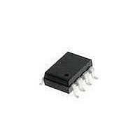
HCPL-4731#320 Avago Technologies US Inc., HCPL-4731#320 Datasheet - Page 12

HCPL-4731#320
Manufacturer Part Number
HCPL-4731#320
Description
OPTOCOUPLER 2CH HS UL 8-SMD GW
Manufacturer
Avago Technologies US Inc.
Datasheet
1.HCPL-073A-000E.pdf
(17 pages)
Specifications of HCPL-4731#320
Input Type
DC
Package / Case
8-SMD Gull Wing
Voltage - Isolation
5000Vrms
Number Of Channels
2, Unidirectional
Current - Output / Channel
60mA
Data Rate
100KBd
Propagation Delay High - Low @ If
65µs @ 40µA
Current - Dc Forward (if)
5mA
Output Type
Open Collector
Mounting Type
Surface Mount, Gull Wing
Isolation Voltage
3750 Vrms
Minimum Forward Diode Voltage
1.1 V
Output Device
Photodarlington
Configuration
2 Channel
Current Transfer Ratio
25000 %
Maximum Baud Rate
100 KBps
Maximum Forward Diode Voltage
1.4 V
Maximum Reverse Diode Voltage
2.5 V
Maximum Input Diode Current
10 mA
Maximum Power Dissipation
115 mW
Maximum Operating Temperature
+ 85 C
Minimum Operating Temperature
- 40 C
Lead Free Status / RoHS Status
Contains lead / RoHS non-compliant
Available stocks
Company
Part Number
Manufacturer
Quantity
Price
12
Notes:
Figure 2. DC Transfer Characteristics
(I
Figure 5. Output Current vs. Input
Diode Forward Current.
1. Specification information is available
2. DC CURRENT TRANSFER RATIO is
3. Device considered a two terminal
4. In accordance with UL 1577, each
4a. In accordance with UL 1577, each
F
I
F
27
24
21
18
15
12
= 0.5 mA to 2.5 mA).
form the factory for 1.6 V operation.
Call your local field sales office for
further information.
defined as the ratio of output
collector current, I
LED input current, I
device: pins 1, 2, 3, and 4 shorted
together, and pins 5, 6, 7, and 8
shorted together.
optocoupler is proof tested by
applying an insulation test voltage
detection current limit, I
optocoupler is proof tested by
applying an insulation test voltage
9
6
3
0
9
8
7
6
5
4
3
2
1
0
– INPUT DIODE FORWARD CURRENT – mA
0
0
4500 V
6000 V
T
V
V
V
A
CC
O
CC
V
= 25°C
O
0.1
= 0.4 V
= 5 V
= 5 V
RMS
RMS
– OUTPUT VOLTAGE – V
for 1 second (leakage
for 1 second (leakage
0.2
70°C
1.0
O
25°C
, to the forward
F
0.3
, times 100%.
I-O
0°C
0.4
5 A.
2.0
0.5
Figure 6. Input Diode Forward
Current vs. Forward Voltage.
Figure 3. DC Transfer Characteristics
(I
5. Measured between pins 1 and 2
6. Common transient immunity in a
0.01
F
100
1.0
0.1
10
7
6
5
4
3
2
1
0
= 50 A to 250 A).
detection current limit, I
This test is performed before the
100% production test for partial
discharge (Method b) shown in the
IEC/EN/DIN EN 60747-5-2 Insulation
Characteristics Table.
shorted together, and pins 3 and 4
shorted together.
Logic High level is the maximum
tolerable (positive) dV
leading edge of the common mode
pulse, V
will remain in a Logic High state (i.e.,
V
immunity in a Logic Low level is he
maximum tolerable (negative)
dV
common mode pulse, V
that the output will remain in a Logic
Low state (i.e., V
O
0
0.8
T
V
CM
> 2.0 V). Common transient
A
CC
= 25°C
/dt on the trailing edge of the
0.9
V
= 5 V
V
O
CM
F
– OUTPUT VOLTAGE – V
V
– FORWARD VOLTAGE
1.0
, to assure that the output
F
+
–
I
F
1.1
1.0
O
< 0.8 V).
1.2
T
CM
A
CM
= 25°C
1.3
I-O
/dt on the
, to assure
1.4
5 A.
2.0
1.5
10. Use of resistor between pins 5 and 7
11. The Applications Information section
Figure 4. Current Transfer Ratio vs.
Forward Current.
Figure 7. Propagation Delay vs.
Temperature.
7. In applications where dV/dt may
8. Use of a 0.1 F bypass capacitor con-
9. Pin 7 open for single channel product.
1.25
0.75
0.25
1.0
0.5
70
60
50
40
30
20
10
exceed 50,000 V/ s (such as static
discharge) a series resistor, R
should be included to protect the
detector IC form destructively high
surge currents. The recommended
value is R
nected between pins 8 and 5 adjacent
to the device is recommended.
will decrease gain and delay time.
Significant reduction in overall gain
can occur when using resistor values
below 47 k
product.
of this data sheet references the
HCPL-47XX part family, but applies
equally to the HCPL-070A and HCPL-
073A parts.
0
0
0.01
0
I
I
R
F
F
10
L
– FORWARD CURRENT – mA
= 0.5 mA
T
= 4.7 k
A
CC
– TEMPERATURE – °C
20
0°C
0.1
= 220
for single channel
25°C
30
70°C
t
t
PLH
PHL
40
.
NORMALIZED
I
V
V
1.0
F
O
CC
= 40 A
50
= 0.4 V
= 5 V
60
CC
,
10
70


