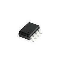
HCPL-4731#320 Avago Technologies US Inc., HCPL-4731#320 Datasheet - Page 9

HCPL-4731#320
Manufacturer Part Number
HCPL-4731#320
Description
OPTOCOUPLER 2CH HS UL 8-SMD GW
Manufacturer
Avago Technologies US Inc.
Datasheet
1.HCPL-073A-000E.pdf
(17 pages)
Specifications of HCPL-4731#320
Input Type
DC
Package / Case
8-SMD Gull Wing
Voltage - Isolation
5000Vrms
Number Of Channels
2, Unidirectional
Current - Output / Channel
60mA
Data Rate
100KBd
Propagation Delay High - Low @ If
65µs @ 40µA
Current - Dc Forward (if)
5mA
Output Type
Open Collector
Mounting Type
Surface Mount, Gull Wing
Isolation Voltage
3750 Vrms
Minimum Forward Diode Voltage
1.1 V
Output Device
Photodarlington
Configuration
2 Channel
Current Transfer Ratio
25000 %
Maximum Baud Rate
100 KBps
Maximum Forward Diode Voltage
1.4 V
Maximum Reverse Diode Voltage
2.5 V
Maximum Input Diode Current
10 mA
Maximum Power Dissipation
115 mW
Maximum Operating Temperature
+ 85 C
Minimum Operating Temperature
- 40 C
Lead Free Status / RoHS Status
Contains lead / RoHS non-compliant
Available stocks
Company
Part Number
Manufacturer
Quantity
Price
9
Absolute Maximum Ratings
(No Derating Required up to 70 C)
Recommended Operating Conditions
*See Note 1.
Storage Temperature
Operating Temperature
Average Forward Input Current (HCPL-4701/4731)
Average Forward Input Current (HCPL-070A/073A)
Peak Transient Input Current (HCPL-4701/4731)
(50% Duty Cycle, 1 ms Pulse Width)
Peak Transient Input Current (HCPL-070A/073A)
(50% Duty Cycle, 1 ms Pulse Width)
Reverse Input Voltage
Input Power Dissipation (Each Channel)
Output Current (Each Channel)
Emitter Base Reverse Voltage (HCPL-4701/070A)
Output Transistor Base Current (HCPL-4701/070A)
Supply Voltage
Output Voltage
Output Power Dissipation (Each Channel)
Total Power Dissipation (Each Channel)
Lead Solder Temperature (for Through Hole Devices)
Reflow Temperature Profile
(for SOIC-8 and Option #300)
Power Supply Voltage
Forward Input Current (ON)
Forward Input Voltage (OFF)
Operating Temperature
Parameter
Parameter
Symbol
V
I
V
F(OFF)
F(ON)
CC
T
A
*
Symbol
I
I
260 C for 10 sec., 1.6 mm below seating plane
F(AVG)
F(AVG)
I
I
V
V
T
T
FPK
FPK
V
V
P
P
I
See Package Outline Drawings section
P
I
CC
EB
O
B
O
O
A
R
S
T
I
Min.
1.6
40
0
0
Minimum
-0.5
-0.5
-55
-40
Max.
5000
0.8
18
70
Maximum
125
100
115
2.5
0.5
85
10
20
10
15
60
18
18
5
5
Units
V
V
C
A
Units
mW
mW
mW
mA
mA
mA
mA
mA
mA
V
V
V
V
C
C


