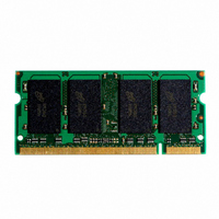
MT8VDDT3264HG-335G3 Micron Technology Inc, MT8VDDT3264HG-335G3 Datasheet - Page 19

MT8VDDT3264HG-335G3
Manufacturer Part Number
MT8VDDT3264HG-335G3
Description
MODULE DDR SDRAM 256MB 200SODIMM
Manufacturer
Micron Technology Inc
Datasheet
1.MT8VDDT3264HG-335G3.pdf
(28 pages)
Specifications of MT8VDDT3264HG-335G3
Memory Type
DDR SDRAM
Memory Size
256MB
Speed
167MHz
Package / Case
200-SODIMM
Lead Free Status / RoHS Status
Contains lead / RoHS non-compliant
Other names
557-1123
pdf: 09005aef8092973f, source: 09005aef80921669
DD8C16_32_64x64HG.fm - Rev. B 9/04 EN
22. The valid data window is derived by achieving
23. Each byte lane has a corresponding DQS.
24. This limit is actually a nominal value and does not
25. To maintain a valid level, the transitioning edge of
512MB); burst refreshing or posting by the DRAM
controller greater than eight refresh cycles is not
allowed.
other specifications:
(
directly porportional with the clock duty cycle
and a practical data valid window can be derived.
The clock is allowed a maximum duty cycle varia-
tion of 45/55, beyond which functionality is
uncertain. Figure 7, Derating Data Valid Window
(
cycles ranging between 50/50 and 45/55.
result in a fail value. CKE is HIGH during RE-
FRESH command period (
LOW (i.e., during standby).
the input must:
t
t
3.8
3.6
3.4
3.2
3.0
2.8
2.6
2.4
2.2
2.0
1.8
QH =
QH -
t
t
DQSQ), shows the derating curves for duty
50/50
HP -
3.750
2.500
t
QHS). The data valid window derates
NA
49.5/50.5
3.700
-335 @
-262/-26A/-265 @
-262/-26A/-265 @
2.463
t
HP (
t
CK = 6ns
t
Figure 7: Derating Data Valid Window
t
3.650
49/51
CK/2),
RFC [MIN]) else CKE is
2.425
t
t
CK = 10ns
CK = 7.5ns
t
DQSQ, and
48.5/52.5
3.600
2.388
48/52
3.550
(
t
t
QH
QH -
2.350
Clock Duty Cycle
19
t
DQSQ)
47.5/53.5
3.500
26. JEDEC specifies CK and CK# input slew rate must
27. DQ and DM input slew rates must not deviate
28. V
29. The clock is allowed up to ±150ps of jitter. Each
128MB, 256MB, 512MB (x64, SR)
2.313
be 1V/ns (2V/ns differentially).
from DQS by more than 10 percent. If the DQ/
DM/DQS slew rate is less than 0.5 V/ns, timing
must be derated: 50ps must be added to
t
slew rate exceeds 4 V/ns, functionality is uncer-
tain. For -335, slew rates must be 0.5 V/ns.
not active while any device bank is active.
timing parameter is allowed to vary by the same
amount.
a. Sustain a constant slew rate from the current
b. Reach at least the target AC level.
c. After the AC target level is reached, continue to
DH for each 100mv/ns reduction in slew rate. If
Micron Technology, Inc., reserves the right to change products or specifications without notice.
DD
AC level through to the target AC level, V
or V
maintain at least the target DC level, V
or V
3.450
47/53
must not vary more than 4 percent if CKE is
2.275
IH
IH
(AC).
(DC).
46.5/54.5
200-PIN DDR SODIMM
3.400
2.238
3.350
46/54
©2004 Micron Technology, Inc. All rights reserved.
2.200
45.5/55.5
3.300
2.163
3.250
45/55
t
DS and
IL
IL
2.125
(DC)
(AC)


