MT18VDDF12872HG-335F1 Micron Technology Inc, MT18VDDF12872HG-335F1 Datasheet
MT18VDDF12872HG-335F1
Specifications of MT18VDDF12872HG-335F1


Related parts for MT18VDDF12872HG-335F1


MT18VDDF12872HG-335F1 Summary of contents
Page 1
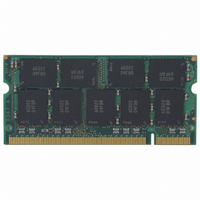
DDR SDRAM SODIMM MT18VDDF12872H – 1GB For component data sheets, refer to Micron’s Web site: Features • 200-pin, small-outline dual in-line memory module (SODIMM) • Fast data transfer rates: PC2100, PC2700, or PC3200 • 1GB (128 Meg x 72) • ...
Page 2
... MT18VDDF12872HG-40B__ MT18VDDF12872HY-40B__ MT18VDDF12872HG-335__ MT18VDDF12872HY-335__ MT18VDDF12872HG-26A__ MT18VDDF12872HG-265__ Notes: 1. Data sheet for the base device can be found on Micron’s Web site. 2. All part numbers end with a two-place code (not shown) that designates component and PCB revisions. Consult factory for current revision codes. Example: MT18VDDF12872HY-335F1. ...
Page 3
Pin Assignments and Descriptions Table 4: Pin Assignments 200-Pin SODIMM Front Pin Symbol Pin Symbol Pin Symbol Pin Symbol 101 REF DQ19 103 SS 5 DQ0 55 DQ24 105 7 DQ1 57 ...
Page 4
Table 5: Pin Descriptions Symbol A0–A12 BA0, BA1 CK0, CK0#, CK1, CK1# CK2, CK2# CKE0, CKE1 DM0–DM8 S0#, S1# SA0–SA2 SCL WE#, CAS#, RAS# CB0–CB7 DQ0–DQ63 DQS0–DQS8 SDA DDSPD V REF PDF: 09005aef80e4880c/Source: 09005aef80e487d7 ...
Page 5
Functional Block Diagram Figure 2: Functional Block Diagram S1# S0# DQS0 DM0 DM CS# DQS DQ0 DQ DQ1 DQ DQ2 DQ DQ3 DQ DQ4 DQ DQ5 DQ DQ6 DQ DQ7 DQ DQS2 DM2 DM CS# DQS DQ16 DQ DQ17 DQ ...
Page 6
... The double data rate architecture is essentially a 2n-prefetch architecture with an interface designed to transfer two data words per clock cycle at the I/O pins. A single read or write access for DDR SDRAM modules effectively consists of a single 2n-bit wide, one-clock-cycle data transfer at the internal DRAM core and two corresponding n-bit wide, one-half-clock-cycle data transfers at the I/O pins ...
Page 7
... Simulations are significantly more accurate and realistic than a gross estimation of module capacitance when inductance and delay parameters associated with trace lengths are used in simulations. JEDEC modules are currently designed using simulations to close timing budgets. Component AC Timing and Operating Conditions Recommended AC operating conditions are given in the DDR component data sheets. Component specifications are available on Micron’ ...
Page 8
I Specifications DD Table 8: I Specifications and Conditions – 1GB DD Values are shown for the 512Mb (64 Meg x 8) component data sheet Parameter/Condition Operating one bank active-precharge current: One device t t bank; Active-precharge ...
Page 9
Serial Presence-Detect Table 9: Serial Presence-Detect EEPROM DC Operating Conditions Parameter/Condition Supply voltage Input high voltage: Logic 1; All inputs Input low voltage: Logic 0; All inputs Output low voltage 3mA OUT Input leakage current GND ...
Page 10
Module Dimensions Figure 3: 200-Pin SODIMM 2.0 (0.079 (2X) 1.8 (0.071) U5 (2X) 6.0 (0.236) TYP 2.44 (0.096) TYP 2.0 (0.079) TYP Pin 1 U11 U15 Pin 200 Notes: 1. All dimensions are in millimeters (inches); MAX/MIN or ...