MT9HTF6472AY-667D4 Micron Technology Inc, MT9HTF6472AY-667D4 Datasheet
MT9HTF6472AY-667D4
Specifications of MT9HTF6472AY-667D4
MT9HTF6472AY-667D4


Related parts for MT9HTF6472AY-667D4


MT9HTF6472AY-667D4 Summary of contents
Page 1
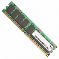
... Gold edge contacts • Single rank pdf: 09005aef80e6f860, source: 09005aef80e5b799 HTF9C32_64_128x72AG_1.fm - Rev. C 6/05 EN Products and specifications discussed herein are subject to change by Micron without notice. ® Web site: www.micron.com/products/modules Figure 1: Height 1.18in. (29.97mm) Options • Package 240-pin DIMM (lead-free) • Frequency/CAS Latency 3ns @ (DDR2-667) 3 ...
Page 2
... MT9HTF12872AY-667__ 1GB MT9HTF12872AY-53E__ 1GB 1GB MT9HTF12872AY-40E__ Notes: 1. All part numbers end with a two-place code (not shown), designating component and PCB revisions. Consult factory for current revision codes. Example: MT9HTF6472AY-40EC2. pdf: 09005aef80e6f860, source: 09005aef80e5b799 HTF9C32_64_128x72AG_1.fm - Rev. C 6/05 EN 256MB 8K 8K (A0–A12) 4 (BA0, BA1) ...
Page 3
SR, ECC) 240-Pin DDR2 SDRAM UDIMM Table of Contents Features . . . . . . . . . . . . . . . . . . . . . . . . . . ...
Page 4
SR, ECC) 240-Pin DDR2 SDRAM UDIMM List of Figures Figure 1: 240-Pin DIMM (MO-237 R/C “A” ...
Page 5
SR, ECC) 240-Pin DDR2 SDRAM UDIMM List of Tables Table 1: Address Table . . . . . . . . . . . . . . . . . . . . . . . ...
Page 6
SR, ECC) 240-Pin DDR2 SDRAM UDIMM Pin Assignments and Descriptions Table 4: Pin Assignment 240-Pin DIMM Front Pin Symbol Pin Symbol Pin Symbol Pin Symbol Pin Symbol Pin Symbol Pin Symbol Pin Symbol ...
Page 7
SR, ECC) 240-Pin DDR2 SDRAM UDIMM Table 5: Pin Descriptions Pin numbers may not correlate with symbols; refer to Pin Assignment tables on page 6 for more information Pin Numbers 195 137, 138, 185, 186, 220, ...
Page 8
SR, ECC) 240-Pin DDR2 SDRAM UDIMM Table 5: Pin Descriptions Pin numbers may not correlate with symbols; refer to Pin Assignment tables on page 6 for more information Pin Numbers 10, 12, 13, ...
Page 9
... SR, ECC) 240-Pin DDR2 SDRAM UDIMM Functional Block Diagram Unless otherwise noted, resistor values are 22Ω. Micron module part numbers are explained in the Module Part Numbering Guide a ing.html. Modules use the following DDR2 SDRAM devices: MT47H32M8BP (256MB); MT47H64M8BT (512MB); and MT47H128M8BT (1GB). Figure 3: Functional Block Diagram ...
Page 10
... DQS, and output data is referenced to both edges of DQS, as well as to both edges of CK. Read and write accesses to DDR2 SDRAM modules are burst-oriented; accesses start at a selected location and continue for a programmed number of locations in a programmed sequence. Accesses begin with the registration of an ACTIVE command, which is then followed by a READ or WRITE command ...
Page 11
SR, ECC) 240-Pin DDR2 SDRAM UDIMM Initialization The following sequence is required for power-up and initialization and is shown in Figure 4, DDR2 Power-Up and Initialization, on page 12. 1. Apply power; if CKE is maintained ...
Page 12
SR, ECC) 240-Pin DDR2 SDRAM UDIMM Figure 4: DDR2 Power-Up and Initialization DDL VTD REF Tb0 T0 Ta0 ...
Page 13
SR, ECC) 240-Pin DDR2 SDRAM UDIMM Mode Register (MR) The mode register is used to define the specific mode of operation of the DDR2 SDRAM device. This definition includes the selection of a burst length, burst ...
Page 14
SR, ECC) 240-Pin DDR2 SDRAM UDIMM Figure 5: Mode Register (MR) Definition 256MB Address Bus 512MB Address Bus BA1 15 MR 1GB Address Bus BA2 BA1 M15 pdf: 09005aef80e6f860, ...
Page 15
SR, ECC) 240-Pin DDR2 SDRAM UDIMM Table 6: Burst Definition Burst Length Operating Mode The normal operating mode is selected by issuing a LOAD MODE command with bit M7 set to zero, and all other bits ...
Page 16
SR, ECC) 240-Pin DDR2 SDRAM UDIMM Power-Down Mode Active power-down (PD) mode is defined by bit M12 as shown in Figure 5, Mode Register (MR) Definition, on page 14. PD mode allows the user to determine ...
Page 17
SR, ECC) 240-Pin DDR2 SDRAM UDIMM Figure 6: CAS Latency (CL CK# CK READ NOP COMMAND DQS, DQS CK# CK READ NOP COMMAND DQS, DQS# DQ Burst length = 4 Posted ...
Page 18
SR, ECC) 240-Pin DDR2 SDRAM UDIMM Extended Mode Register (EMR) The extended mode register controls functions beyond those controlled by the mode register; these additional functions are DLL enable/disable, output drive strength, ODT (R ), Posted ...
Page 19
SR, ECC) 240-Pin DDR2 SDRAM UDIMM Figure 7: Extended Mode Register Definition 256MB Address Bus 512MB Address Bus BA1 15 EMR 1GB Address Bus BA2 BA1 EMR E12 E15 E14 ...
Page 20
... ODT for any or all devices. R tance values of 75Ω and 150Ω are selectable and apply to each DQ, DQS/DQS#, RDQS/ RDQS#, and DM signals. Additionally, the -667 speed modules offer a third option of 50Ω. Reserved states should not be used, as unknown operation or incompatibility with future versions may result ...
Page 21
SR, ECC) 240-Pin DDR2 SDRAM UDIMM additive latency (AL) and CAS Latency (CL CL. Write latency (WL) is equal to READ latency minus one clock ...
Page 22
SR, ECC) 240-Pin DDR2 SDRAM UDIMM Extended Mode Register 2 (EMR2) The Extended Mode Register 2 (EMR2) controls functions beyond those controlled by the mode register. Currently all bits in EMR2 are reserved as shown in ...
Page 23
SR, ECC) 240-Pin DDR2 SDRAM UDIMM Extended Mode Register 3 (EMR3) The Extended Mode Register 3 (EMR3) controls functions beyond those controlled by the mode register. Currently all bits in EMR3 are reserved as shown in ...
Page 24
SR, ECC) 240-Pin DDR2 SDRAM UDIMM Command Truth Tables Table 7, Commands Truth Table provides a quick reference of DDR2 SDRAM device available commands. Refer to the 256Mb, 512Mb, or 1Gb DDR2 SDRAM component data sheet ...
Page 25
SR, ECC) 240-Pin DDR2 SDRAM UDIMM Absolute Maximum Ratings Stresses greater than those listed may cause permanent damage to the device. This is a stress rating only, and functional operation of the device at these or ...
Page 26
SR, ECC) 240-Pin DDR2 SDRAM UDIMM Input Electrical Characteristics and Operating Conditions Table 10: Input DC Logic Levels All voltages referenced to V Parameter Input High (Logic 1) Voltage Input Low (Logic 0) Voltage Table 11: ...
Page 27
... Simulations can then render a con- siderably more accurate result. JEDEC modules are now designed by using simulations to close timing budgets. pdf: 09005aef80e6f860, source: 09005aef80e5b799 HTF9C32_64_128x72AG_2.fm - Rev Timing Patterns – ...
Page 28
SR, ECC) 240-Pin DDR2 SDRAM UDIMM Table 15: DDR2 I Specifications and Conditions – 256MB DD Values shown for DDR2 SDRAM components only Parameter/Condition Operating one device bank active-precharge current ...
Page 29
SR, ECC) 240-Pin DDR2 SDRAM UDIMM Table 16: DDR2 I Specifications and Conditions – 512MB DD Values shown for DDR2 SDRAM components only Parameter/Condition Operating one device bank active-precharge current ...
Page 30
SR, ECC) 240-Pin DDR2 SDRAM UDIMM Table 17: DDR2 I Specifications and Conditions – 1GB DD Values shown for DDR2 SDRAM components only Parameter/Condition Operating one device bank active-precharge current ...
Page 31
SR, ECC) 240-Pin DDR2 SDRAM UDIMM AC Timing and Operating Conditions Table 18: AC Operating Conditions (Sheet Notes: 1–5; notes appear on page 35; 0°C ≤ Characteristics Parameter ...
Page 32
SR, ECC) 240-Pin DDR2 SDRAM UDIMM Table 18: AC Operating Conditions (Sheet Notes: 1–5; notes appear on page 35; 0°C ≤ Characteristics Parameter DQS input high pulse width DQS input low ...
Page 33
SR, ECC) 240-Pin DDR2 SDRAM UDIMM Table 18: AC Operating Conditions (Sheet Notes: 1–5; notes appear on page 35; 0°C ≤ Characteristics Parameter Address and control input pulse width for each ...
Page 34
SR, ECC) 240-Pin DDR2 SDRAM UDIMM Table 18: AC Operating Conditions (Sheet Notes: 1–5; notes appear on page 35; 0°C ≤ Characteristics Parameter ODT turn-on delay ODT turn-on ODT turn-off delay ...
Page 35
SR, ECC) 240-Pin DDR2 SDRAM UDIMM Notes 1. All voltages referenced Tests for AC timing, nominal reference/supply voltage levels, but the related specifications and device operation are guaranteed for the full voltage range ...
Page 36
SR, ECC) 240-Pin DDR2 SDRAM UDIMM 13 recommended that DQS be valid (HIGH or LOW before the WRITE com- mand. The case shown (DQS going from High-Z to logic LOW) applies when ...
Page 37
SR, ECC) 240-Pin DDR2 SDRAM UDIMM t 32. RPA timing applies when the PRECHARGE(ALL) command is issued, regardless of the number of banks already open or closed single-bank PRECHARGE command is issued, 33. Value ...
Page 38
SR, ECC) 240-Pin DDR2 SDRAM UDIMM Serial Presence-Detect SPD Clock and Data Conventions Data states on the SDA line can change only during SCL LOW. SDA state changes during SCL HIGH are reserved for indicating start ...
Page 39
SR, ECC) 240-Pin DDR2 SDRAM UDIMM Figure 13: Definition of Start and Stop SCL SDA Figure 14: Acknowledge Response From Receiver SCL from Master Data Output from Transmitter Data Output from Receiver pdf: 09005aef80e6f860, source: 09005aef80e5b799 ...
Page 40
SR, ECC) 240-Pin DDR2 SDRAM UDIMM Table 19: EEPROM Device Select Code The most significant bit (b7) is sent first Select Code Memory Area Select Code (two arrays) Protection Register Select Code Table 20: EEPROM Operating ...
Page 41
SR, ECC) 240-Pin DDR2 SDRAM UDIMM Table 21: Serial Presence-Detect EEPROM DC Operating Conditions All voltages referenced to V Parameter/Condition Supply Voltage Input High Voltage: Logic 1; All inputs Input Low Voltage: Logic 0; All inputs ...
Page 42
SR, ECC) 240-Pin DDR2 SDRAM UDIMM Table 23: Serial Presence-Detect Matrix “1”/“0”: Serial Data, “driven to HIGH”/“driven to LOW” Byte Description 0 Number of SPD Bytes Used by Micron 1 Total Number of Bytes in SPD ...
Page 43
SR, ECC) 240-Pin DDR2 SDRAM UDIMM Table 23: Serial Presence-Detect Matrix “1”/“0”: Serial Data, “driven to HIGH”/“driven to LOW” Byte Description 32 Address and Command Setup Time, 33 Address and Command Hold Time, 34 Data/ Data ...
Page 44
SR, ECC) 240-Pin DDR2 SDRAM UDIMM Module Dimensions All dimensions are in inches (millimeters); The dimensional diagram is for reference only. Refer to the MO document for complete design dimensions. Figure 16: 240-pin DIMM DDR2 Module ...