HDSP-2533 Avago Technologies US Inc., HDSP-2533 Datasheet - Page 10
HDSP-2533
Manufacturer Part Number
HDSP-2533
Description
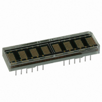
LED DISPLAY 5X7 8CHAR 5MM GREEN
Manufacturer
Avago Technologies US Inc.
Series
HDSP-253xr
Datasheet
1.HDSP-2533.pdf
(15 pages)
Specifications of HDSP-2533
Display Type
Alphanumeric
Common Pin
*
Package / Case
28-DIP
Color
Green
Size / Dimension
1.69" x .45" (42.9mm x 11.4mm)
Number Of Digits/alpha
8
Digit/alpha Size
0.20" (5mm)
Number Of Digits
8
Character Size
2.54 mm x 4.57 mm
Illumination Color
Green
Wavelength
574 nm
Operating Voltage
5 V
Operating Current
370 mA
Maximum Operating Temperature
+ 85 C
Minimum Operating Temperature
- 40 C
Luminous Intensity
7.5 ucd
Viewing Area (w X H)
40.06 mm x 4.57 mm
Lead Free Status / RoHS Status
Lead free / RoHS Compliant
Lead Free Status / RoHS Status
Lead free / RoHS Compliant, Lead free / RoHS Compliant
Other names
516-1169-5


UDC RAM and UDC Address Register
Figure 3 shows the logic levels needed to access the UDC
RAM and the UDC Address Register. The UDC Address
Register is eight bits wide. The lower four bits (D
used to select one of the 16 UDC locations. The upper four
bits (D
stored in the UDC Address Register, the UDC RAM can be
accessed.
To completely specify a 5 x 7 character requires eight write
cycles. One cycle is used to store the UDC RAM address in
the UDC Address Register. Seven cycles are used to store
dot data in the UDC RAM. Data is entered by rows. One
cycle is needed to access each row. Figure 4 shows the
organization of a UDC character assuming the symbol to
be stored is an “F. ” A
accessed and D
The upper three bits (D
cant bit) corresponds to the right most column of the 5 x 7
matrix and D
most column of the 5 x 7 matrix.
Flash RAM
Figure 5 shows the logic levels needed to access the Flash
RAM. The Flash RAM has one bit associated with each
location of the Character RAM. The Flash input is used
to select the Flash RAM. Address lines A
Address lines A
Flash RAM to store the attribute. D
remove the flash attribute. D
and D
When the attribute is enabled through bit 3 of the Control
Word and a “1” is stored in the Flash RAM, the correspond-
ing character will flash at approximately 2 Hz. The actual
rate is dependent on the clock frequency. For an external
clock the flash rate can be calculated by dividing the clock
frequency by 28,672.
C C C C C
O O O O O
L L L L L
1 2 3 4 5
D
1 1 1 1 1
1 0 0 0 0
1 0 0 0 0
1 1 1 1 0
1 0 0 0 0
1 0 0 0 0
1 0 0 0 0
IGNORED
Figure 4. Data to load “”F’’ into the UDC RAM.
10
4
D
0 = LOGIC 0; 1 = LOGIC 1; * = ILLUMINATED LED
3
D
0
2
4
= “0” removes the attribute.
-D
D
1
7
D
) are not used. Once the UDC address has been
0
4
(most significant bit) corresponds to the left
0
0
-D
-A
ROW 1
ROW 2
ROW 3
ROW 4
ROW 5
ROW 6
ROW 7
2
4
are used to select the location in the
are used to transmit the row dot data.
0
-A
5
2
-D
are used to select the row to be
UDC CHARACTER
• • • • •
•
•
• • • •
•
•
•
7
) are ignored. D
0
= “1” stores the attribute
0
is used to store or
HEX CODE
1F
10
10
1E
10
10
10
3
-A
0
4
(least signifi-
are ignored.
0
-D
3
) are
CONTROL SIGNALS
UDC ADDRESS REGISTER ADDRESS
UDC ADDRESS REGISTER DATA FORMAT
CONTROL SIGNALS
UDC RAM ADDRESS
UDC RAM
DATA FORMAT
0 = LOGIC 0; 1 = LOGIC 1; X = DO NOT CARE
Figure 3. Logic levels to access a UDC character.
CONTROL SIGNALS
FLASH RAM ADDRESS
FLASH RAM DATA FORMAT
0 = LOGIC 0; 1 = LOGIC 1; X = DO NOT CARE
Figure 5. Logic levels to access the Flash RAM.
RST
RST
RST
FL
D
D
D
FL
FL
1
0
X
1
1
X
1
1
X
7
7
7
CE
A
D
0
X
X
CE
CE
A
D
A
D
0
0
X
0
0
X
4
6
4
6
4
6
WR
A
D
0
0
1
1
X
X
WR
WR
3
5
A
D
A
D
0
0
1
1
0
0
0
1
1
1
X
X
3
3
5
5
RD
A
D
0
1
0
1
X
2
4
RD
RD
CHARACTER
A
A
D
D
0
1
0
1
X
0
1
0
1
C
O
L
1
X
ADDRESS
2
2
4
4
ROW SELECT
UNDEFINED
WRITE TO DISPLAY
READ FROM DISPLAY
UNDEFINED
A
D
X
1
3
UNDEFINED
WRITE TO DISPLAY
READ FROM DISPLAY
UNDEFINED
UNDEFINED
WRITE TO DISPLAY
READ FROM DISPLAY
UNDEFINED
A
A
D
D
X
1
1
3
3
DOT DATA
A
D
X
0
2
A
UDC CODE
A
D
D
X
0
0
2
2
000 = LEFT MOST
111 = RIGHT MOST
D
X
1
000 = ROW 1
110 = ROW 7
D
D
1
1
D
0
1
0
D
D
C
O
L
5
REMOVE FLASH AT
SPECIFIED DIGIT LOCATION
STORE FLASH AT
SPECIFIED DIGIT LOCATION
0
0
Related parts for HDSP-2533
Image
Part Number
Description
Manufacturer
Datasheet
Request
R

Part Number:
Description:
LED 7-SEG 7.6MM CC HE RED RHD
Manufacturer:
Avago Technologies US Inc.
Datasheet:

Part Number:
Description:
LED 7-SEG 7.6MM CA HE RED RHD
Manufacturer:
Avago Technologies US Inc.
Datasheet:

Part Number:
Description:
Seven-Segment Numeric LED Display,2-CHARACTER,Red,DIP
Manufacturer:
Avago Technologies US Inc.
Datasheet:

Part Number:
Description:
Seven-Segment Numeric LED Display,2-CHARACTER,Green,DIP
Manufacturer:
Avago Technologies US Inc.
Datasheet:
Part Number:
Description:
Seven-Segment Numeric LED Display,2-CHARACTER,Green,DIP
Manufacturer:
Avago Technologies US Inc.
Datasheet:
Part Number:
Description:
Seven-Segment Numeric LED Display,2-CHARACTER,Red,DIP
Manufacturer:
Avago Technologies US Inc.
Datasheet:
Part Number:
Description:
Seven-Segment Numeric LED Display,2-CHARACTER,Green,DIP
Manufacturer:
Avago Technologies US Inc.
Datasheet:

Part Number:
Description:
Seven-Segment Numeric LED Display,2-CHARACTER,Orange-Red,DIP
Manufacturer:
Avago Technologies US Inc.
Datasheet:

Part Number:
Description:
LED 7-SEG 14.2MM 2DIG CC HER RHD
Manufacturer:
Avago Technologies US Inc.
Datasheet:

Part Number:
Description:
LED 7-SEG 14.2MM 2DIG CC HER RHD
Manufacturer:
Avago Technologies US Inc.
Datasheet:

Part Number:
Description:
LED 7-SEG 14.2MM 2DIG CA HER RHD
Manufacturer:
Avago Technologies US Inc.
Datasheet:

Part Number:
Description:
LED 7-SEG 14.2MM 2DIG CA GRN RHD
Manufacturer:
Avago Technologies US Inc.
Datasheet:

Part Number:
Description:
LED 7-SEG 14.2MM 2DIG CC GRN RHD
Manufacturer:
Avago Technologies US Inc.
Datasheet:

Part Number:
Description:
LED 7-SEG 14.2MM 2DIG CA GRN RHD
Manufacturer:
Avago Technologies US Inc.
Datasheet:

Part Number:
Description:
LED 7-SEG 14.2MM 2DIG CC GRN RHD
Manufacturer:
Avago Technologies US Inc.
Datasheet: