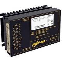
LK5660-7R POWER ONE, LK5660-7R Datasheet - Page 24
LK5660-7R
Manufacturer Part Number
LK5660-7R
Description
CONVERTER AC/DC 225VIN 48VOUT
Manufacturer
POWER ONE
Series
Kr
Datasheet
1.LK5660-7R.pdf
(29 pages)
Specifications of LK5660-7R
Voltage - Output
24V
Number Of Outputs
2
Power (watts)
150W
Applications
Commercial
Power Supply Type
Switching (Closed Frame)
Voltage - Input
85 ~ 255VAC
Mounting Type
Chassis Mount
1st Output
24 VDC @ 3A
2nd Output
24 VDC @ 3A
Size / Dimension
6.63" L x 4.37" W x 3.15" H (168.5mm x 111mm x 80mm)
Power (watts) - Rated
150W
Operating Temperature
-25°C ~ 71°C
Efficiency
83%
Approvals
CE, cUL, EN, TUV
Output Voltage (channel 1)
24 V
Output Current (channel 1)
3 A
Output Voltage (channel 2)
24 V
Output Current (channel 2)
3 A
Isolation Voltage
2.8 KV
Output Type
Isolated
Lead Free Status / RoHS Status
Contains lead / RoHS non-compliant
3rd Output
-
4th Output
-
Lead Free Status / Rohs Status
Lead free / RoHS Compliant
Other names
LK 5660-7R
LK 5660-7R
Q1660869
LK 5660-7R
Q1660869


D Undervoltage Monitor
The input and/or output undervoltage monitoring circuit
operates independently of the built-in input undervoltage
lockout circuit. A logic "low" (self conducting JFET) or "high"
signal (NPN output) is generated at the D output (pin 20),
when one of the monitored voltages drops below the
preselected threshold level V
S– / Vo1–. The D output recovers, when the monitored
voltages exceed V
in the factory. The threshold level V
potentiometer accessible through a hole in the front cover,
or adjusted in the factory to a fixed value specified by the
customer.
Option D exists in various versions D0 – DD, as shown in
the table below.
JFET output (D0 – D4):
Pin D is internally connected via the drain-source path of a
JFET (self-conducting type) to the negative potential of
output 1. V
voltage level (V
JFET should not exceed 2.5 mA. The JFET is protected by
a 0.5 W Zener diode of 8.2 V against external overvoltages.
Table 21: Undervoltage monitoring functions
1
Fig. 38
Option D0 – D4: JFET output, I
BCD20001-G Rev AC, 16-Dec-2010
Threshold level adjustable by potentiometer. See Output Data for V
2
3
4
JFET
Fixed value. Tracking if V
The threshold level permanently adjusted according to customer specification ±2% at 25 °C. Any value within the specified range
is basically possible, but causes a special type designation in addition to the standard option designations (D0/D9).
V
remain powered during nearly the full hold-up time t
D1
D2
D3
D4
D0
b
Output type
is the voltage generated by the boost regulator. When V
D
0.4 V (logic low) corresponds to a monitored
Self-conducting
junction FET
NPN
i
DD
D5
D6
D7
D8
D9
and/or V
t
+ V
h
. The threshold level V
o1
yes
yes
yes
yes
V
o1
) V
no
no
no
Monitoring
b
4
is adjusted via R-input, option P, or sense lines.
t
. This signal is referenced to
t
. The current I
D
11006a
to
V
2.5 mA
yes
yes
yes
yes
yes
yes
o
no
is either adjusted by a
/V
20
14
o1
D
S–/Vo1–
Vo+/Vo1+
I
D
V
D
bi
D
through the
is adjusted
Minimum adjustment range
R
355 VDC
355 VDC
355 VDC
355 VDC
h
.
p
V
tb
of threshold level V
-
-
-
Page 24 of 29
4
b
drops below 355 V, the D signal triggers, and the output(s) will
BR
NPN output (D5 – DD):
Pin D is internally connected via the collector-emitter path
of a NPN transistor to the negative potential of output 1. V
level (V
open collector should not exceed 20 mA. The NPN output
is not protected against external overvoltages. V
not exceed 40 V.
Fig. 39
Option D5 – DD: NPN output, V
Table 22: JFET output (D0 – D4)
Table 23: JFET output (D5 – DD)
V
.
b
0.4 V (logic low) corresponds to a monitored voltage
, V
V
V
(0.95 – 0.985 V
(0.95 – 0.985 V
b
o1
b
V
and V
V
and V
V
150 – 280 Watt AC-DC Converters
i
b
status
b
, V
3.5 – V
3.5 – V
3.5 – V
3.5 – V
b
and/or V
or V
or V
o1
t
o1
V
o1
-
o1
to
status
K Series with PFC Data Sheet
o1
BR
BR
BR
BR
V
V
t
V
1
3
3
1
t
o1
V
+ V
+ V
t
o1
o1
t
)
)
)
NPN open
collector
h
2
2
h
V
t
Typical hysteresis V
+ V
high, H, I
low, L, V
low, L, V
high, H, I
h
. The current I
o1
for V
11007a
D
D
40 V, I
2.5 – 0.6 V
2.5 – 0.6 V
2.5 – 0.6 V
2.5 – 0.6 V
D
D output, V
t min
D output, V
D
14
20
0.4 V at I
25 µA at V
Vo+/Vo1+
D
S–/Vo1–
0.4 V at I
V
"0"
"0"
www.power-one.com
25 µA at V
–
-
ho
V
D
t max
I
D
D
V
ho
20 mA
D
through the
D
D
D
[% of V
D
D
= 2.5 mA
D
= 20 mA
D
= 5.25 V
R
= 40 V
p
should
t
]
D
Related parts for LK5660-7R
Image
Part Number
Description
Manufacturer
Datasheet
Request
R

Part Number:
Description:
SWITCHING POWER SUPPLIES, SINGLE OUTPUT, 80 WATTS
Manufacturer:
POWER ONE
Datasheet:
Part Number:
Description:
HAS SERIES - 30 WATT
Manufacturer:
POWER ONE
Datasheet:
Part Number:
Description:
SINGLE OUTPUT
Manufacturer:
POWER ONE
Datasheet:

Part Number:
Description:
BRS DC/DC converters(1.5 WATT)
Manufacturer:
Power-One
Datasheet:
Part Number:
Description:
3...15 Watt DC-DC Converter
Manufacturer:
Power-One
Datasheet:
Part Number:
Description:
HBS SERIES - 100 WATT
Manufacturer:
Power-One
Datasheet:
Part Number:
Description:
3...15 Watt DC-DC Converter
Manufacturer:
Power-One
Datasheet:
Part Number:
Description:
BUS DC/DC converters(3 WATT)
Manufacturer:
Power-One
Datasheet:
Part Number:
Description:
HES SERIES 150 WATT
Manufacturer:
Power-One
Datasheet:
Part Number:
Description:
1.25 WATT
Manufacturer:
Power-One
Datasheet: