ADZS-21262-1-EZEXT Analog Devices Inc, ADZS-21262-1-EZEXT Datasheet - Page 12
ADZS-21262-1-EZEXT
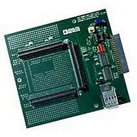
Manufacturer Part Number
ADZS-21262-1-EZEXT
Description
BOARD DAUGHTER FOR ADSP-21262
Manufacturer
Analog Devices Inc
Datasheet
1.ADSP-21363KSWZ-1AA.pdf
(56 pages)
Specifications of ADZS-21262-1-EZEXT
Accessory Type
DSP
Silicon Manufacturer
Analog Devices
Core Architecture
SHARC
Features
Expansion Interface, High Speed Converter (HSC) Interface
Kit Contents
Board Docs
Silicon Family Name
SHARC
Silicon Core Number
ADSP-21262
Rohs Compliant
Yes
Lead Free Status / RoHS Status
Lead free / RoHS Compliant
For Use With/related Products
ADSP-21262
Lead Free Status / RoHS Status
Lead free / RoHS Compliant, Lead free / RoHS Compliant


ADSP-21362/ADSP-21363/ADSP-21364/ADSP-21365/ADSP-21366
Table 6. Pin Descriptions (Continued)
Pin
SPICLK
SPIDS
MOSI
MISO
CLKIN
XTAL
CLK_CFG1–0
The following symbols appear in the Type column of
S = synchronous, (A/D) = active drive, (O/D) = open drain, and T = three-state, (pd) = pull-down resistor, (pu) = pull-up resistor.
Type
I/O
(pu)
I
I/O (O/D)
(pu)
I/O (O/D)
(pu)
I
O
I
State During and
After Reset
Three-state with
pull-up enabled,
driven high in SPI-
master boot mode
Input only
Three-state with
pull-up enabled,
driven low in SPI-
master boot mode
Three-state with
pull-up enabled
Input only
Output only
Input only
2
Rev. G | Page 12 of 56 | March 2011
Table
Function
Serial Peripheral Interface Clock Signal. Driven by the master, this signal controls the
rate at which data is transferred. The master can transmit data at a variety of baud rates.
SPICLK cycles once for each bit transmitted. SPICLK is a gated clock active during data
transfers, only for the length of the transferred word. Slave devices ignore the serial clock
if the slave select input is driven inactive (high). SPICLK is used to shift out and shift in
the data driven on the MISO and MOSI lines. The data is always shifted out on one clock
edge and sampled on the opposite edge of the clock. Clock polarity and clock phase
relative to data are programmable into the SPICTL control register and define the transfer
format. SPICLK has a 22.5 kΩ internal pull-up resistor.
Serial Peripheral Interface Slave Device Select. An active low signal used to select the
processor as an SPI slave device. This input signal behaves like a chip select, and is
provided by the master device for the slave devices. In multimaster mode the processor’s
SPIDS signal can be driven by a slave device to signal to the processor (as SPI master)
that an error has occurred, as some other device is also trying to be the master device. If
asserted low when the device is in master mode, it is considered a multimaster error. For
a single-master, multiple-slave configuration where flag pins are used, this pin must be
tied or pulled high to V
action, any of the master processor’s flag pins can be used to drive the SPIDS signal on
the SPI slave device.
SPI Master Out Slave In. If the ADSP-2136x is configured as a master, the MOSI pin
becomes a data transmit (output) pin, transmitting output data. If the processor is
configured as a slave, the MOSI pin becomes a data receive (input) pin, receiving input
data. In an SPI interconnection, the data is shifted out from the MOSI output pin of the
master and shifted into the MOSI input(s) of the slave(s). MOSI has a 22.5 kΩ internal pull-
up resistor.
SPI Master In Slave Out. If the ADSP-2136x is configured as a master, the MISO pin
becomes a data receive (input) pin, receiving input data. If the processor is configured
as a slave, the MISO pin becomes a data transmit (output) pin, transmitting output data.
In an SPI interconnection, the data is shifted out from the MISO output pin of the slave
and shifted into the MISO input pin of the master. MISO has a 22.5 kΩ internal pull-up
resistor. MISO can be configured as O/D by setting the OPD bit in the SPICTL register.
Note: Only one slave is allowed to transmit data at any given time. To enable broadcast
transmission to multiple SPI slaves, the processor’s MISO pin can be disabled by setting
Bit 5 (DMISO) of the SPICTL register equal to 1.
Local Clock In. Used in conjunction with XTAL. CLKIN is the ADSP-2136x clock input. It
configures the ADSP-2136x to use either its internal clock generator or an external clock
source. Connecting the necessary components to CLKIN and XTAL enables the internal
clock generator. Connecting the external clock to CLKIN while leaving XTAL uncon-
nected configures the processors to use the external clock source such as an external
clock oscillator. The core is clocked either by the PLL output or this clock input depending
on the CLK_CFG1–0 pin settings. CLKIN should not be halted, changed, or operated
below the specified frequency.
Crystal Oscillator Terminal. Used in conjunction with CLKIN to drive an external crystal.
Core to CLKIN Ratio Control. These pins set the start up clock frequency. Note that the
operating frequency can be changed by programming the PLL multiplier and divider in
the PMCTL register at any time after the core comes out of reset. The allowed values are:
00 = 6:1
01 = 32:1
10 = 16:1
11 = reserved.
6: A = asynchronous, G = ground, I = input, O = output, P = power supply,
DDEXT
on the master device. For processor to processor SPI inter-
Related parts for ADZS-21262-1-EZEXT
Image
Part Number
Description
Manufacturer
Datasheet
Request
R

Part Number:
Description:
BOARD DAUGHTER EZ EXTENDER
Manufacturer:
Analog Devices Inc
Datasheet:

Part Number:
Description:
±1.7g Dual-Axis IMEMS Accelerometer Evaluation Board
Manufacturer:
Analog Devices Inc
Datasheet:

Part Number:
Description:
Inertial Sensor Evaluation System
Manufacturer:
Analog Devices Inc
Datasheet:
Part Number:
Description:
Manufacturer:
Analog Devices Inc
Datasheet:
Part Number:
Description:
Manufacturer:
Analog Devices Inc
Datasheet:
Part Number:
Description:
Manufacturer:
Analog Devices Inc
Datasheet:
Part Number:
Description:
Manufacturer:
Analog Devices Inc
Datasheet:
Part Number:
Description:
Manufacturer:
Analog Devices Inc
Datasheet:
Part Number:
Description:
Manufacturer:
Analog Devices Inc
Datasheet:
Part Number:
Description:
Manufacturer:
Analog Devices Inc
Datasheet:
Part Number:
Description:
Manufacturer:
Analog Devices Inc
Datasheet:
Part Number:
Description:
Manufacturer:
Analog Devices Inc
Datasheet:
Part Number:
Description:
Manufacturer:
Analog Devices Inc
Datasheet: