KIT15XS3400EVBE Freescale Semiconductor, KIT15XS3400EVBE Datasheet - Page 4
KIT15XS3400EVBE
Manufacturer Part Number
KIT15XS3400EVBE
Description
BOARD EVALUATION FOR 5XS3400
Manufacturer
Freescale Semiconductor
Type
MOSFET & Power Driverr
Specifications of KIT15XS3400EVBE
Main Purpose
Automotive Lighting
Embedded
No
Utilized Ic / Part
MC15XS3400
Primary Attributes
Four low RDS(ON) MOSFETs
Secondary Attributes
Temperature Protection
Interface Type
SPI
Product
Power Management Modules
Silicon Manufacturer
Freescale
Silicon Core Number
MC15XS3400
Kit Application Type
Power Management
Application Sub Type
EXtreme Switch
Kit Contents
Board, CD
Rohs Compliant
Yes
Lead Free Status / RoHS Status
Lead free / RoHS Compliant
For Use With/related Products
15XS3400


Table 2. 15XS3400 Pin Definitions
4
15XS3400
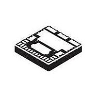
PIN CONNECTIONS
Transparent Top View of Package
Number
A functional description of each pin can be found in the Functional Pin Description section beginning on page 23.
Pin
10
11
12
13
1
2
3
5
6
7
8
9
Pin Name
WAKE
CSNS
SCLK
VDD
RST
IN0
IN1
IN2
IN3
CS
FS
SI
Function
Output
Output
Power
Input
Input
Input
Input
Input
Input
Pin
GND
HS3
SO
Digital Drain Voltage
Output Current
Formal Name
Direct Inputs
(Active Low)
(Active Low)
Fault Status
Serial Clock
13
Chip Select
Serial Input
Monitoring
16
17
18
Wake
Reset
12
Figure 3. 15XS3400 Pin Connections
HS1
19
11
PIN CONNECTIONS
10
9
This pin reports an analog value proportional to the designated HS[0:3] output
current or the temperature of the GND flag (pin 14). It is used externally to
generate a ground-referenced voltage for the microcontroller (MCU) . Current
recopy and temperature feedback is SPI programmable.
Each direct input controls the device mode. The IN[0 : 3] high side input pins
are used to directly control HS0 : HS3 high side output pins.
The PWM frequency can be generated from IN0 pin to PWM module in case
the external clock is set.
This pin is an open drain configured output requiring an external pull-up
resistor to V
This input pin controls the device mode.
This input pin is used to initialize the device configuration and fault registers,
as well as place the device in a low-current Sleep mode.
This input pin is connected to a chip select output of a master microcontroller
(MCU).
This input pin is connected to the MCU providing the required bit shift clock for
SPI communication.
This pin is a command data input pin connected to the SPI serial data output
of the MCU or to the SO pin of the previous device of a daisy
This pin is an external voltage input pin used to supply power interfaces to the
SPI bus.
8
VPWR
GND
14
15
NC
20
7
6
DD
for fault reporting.
5
4
3
HS0
21
2
22
24
23
1
Definition
Analog Integrated Circuit Device Data
FSI
GND
HS2
Freescale Semiconductor
-
chain of devices.
Related parts for KIT15XS3400EVBE
Image
Part Number
Description
Manufacturer
Datasheet
Request
R

Part Number:
Description:
Manufacturer:
Freescale Semiconductor, Inc
Datasheet:
Part Number:
Description:
Manufacturer:
Freescale Semiconductor, Inc
Datasheet:
Part Number:
Description:
Manufacturer:
Freescale Semiconductor, Inc
Datasheet:
Part Number:
Description:
Manufacturer:
Freescale Semiconductor, Inc
Datasheet:
Part Number:
Description:
Manufacturer:
Freescale Semiconductor, Inc
Datasheet:
Part Number:
Description:
Manufacturer:
Freescale Semiconductor, Inc
Datasheet:
Part Number:
Description:
Manufacturer:
Freescale Semiconductor, Inc
Datasheet:
Part Number:
Description:
Manufacturer:
Freescale Semiconductor, Inc
Datasheet:
Part Number:
Description:
Manufacturer:
Freescale Semiconductor, Inc
Datasheet:
Part Number:
Description:
Manufacturer:
Freescale Semiconductor, Inc
Datasheet:
Part Number:
Description:
Manufacturer:
Freescale Semiconductor, Inc
Datasheet:
Part Number:
Description:
Manufacturer:
Freescale Semiconductor, Inc
Datasheet:
Part Number:
Description:
Manufacturer:
Freescale Semiconductor, Inc
Datasheet:
Part Number:
Description:
Manufacturer:
Freescale Semiconductor, Inc
Datasheet:
Part Number:
Description:
Manufacturer:
Freescale Semiconductor, Inc
Datasheet: