EVALSF2-ICE2B765P Infineon Technologies, EVALSF2-ICE2B765P Datasheet - Page 7
EVALSF2-ICE2B765P
Manufacturer Part Number
EVALSF2-ICE2B765P
Description
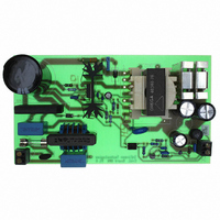
BOARD DEMO ICE2B765P 80W SMPS
Manufacturer
Infineon Technologies
Series
CoolSET®F2r
Datasheet
1.EVALSF2-ICE2B765P.pdf
(23 pages)
Specifications of EVALSF2-ICE2B765P
Main Purpose
AC/DC, Primary Side
Outputs And Type
1, Isolated
Power - Output
80W
Voltage - Output
24V
Current - Output
3.3A
Voltage - Input
85 ~ 270VAC
Regulator Topology
Flyback
Frequency - Switching
67kHz
Board Type
Fully Populated
Utilized Ic / Part
ICE2B765
Lead Free Status / RoHS Status
Lead free / RoHS Compliant
Other names
EVALSF2-ICE2B765PIN


80W 24V Adapter with ICE2B765P on Board
Description
Introduction
The EVALSF2-ICE2B765P demoboard is a low cost flyback switching power supply using the
ICE2B765P integrated circuit from the CoolSET
-F2 family. The circuit shown in
Figure 2
details a
24V, 80W supply that operates from an line input voltage range of 85 to 265V
, suitable for
AC
applications requiring either an open frame supply or an enclosed adapter.
Line Input
The AC line input side comprises of an input fuse F1 as line input over current protection as well as
choke L5 and the X2 capacitors C8 and C24 as radio interference suppressors. R19 prevents the
application against line shut on spikes. After the bridge rectifier BR1 and input capacitor C3, a voltage
from 120 to 380 V
is present. Only a 220µF input capacitor is required due to the wider duty cycle
DC
DC
of the ICE-F2-family.
MAX
Startup
From the line input voltage, the current supply which is used to charge up the chip supply capacitor C4
is derived by using resistors R7 and rectifier diode D10. Because of the very low start up current of
typically 27µA, a high-value resistor can be used to realize the startup.
Note:
Improve your standby power via increasing R7.
Operation Mode
During operation, the V
pin is supplied via a separate transformer winding with associated
CC
rectification D2 and buffering C4 and filter capacitor C20. Resistor R8 is used for current limiting
during the charging of C4. In order not to exceed the maximum voltage at the V
pin an external
CC
zener diode D7 limits this voltage. During light or no load condition the switching frequency is reduced
down to 21kHz in order to reduce the switching losses without audible noise.
Note:
In order to improve the standby power, set the board in the burst mode during no load condition via
increasing the chip supply resistor R8.
Softstart
In order to minimize the electrical stress, a Soft-Start function is realized by an internal resistor and the
adjustable external capacitor C18.
Snubber Network
Due to the high avalanche rugged CoolMOS inside, a simple RCD snubber protection can be used.
The network R10, C12 and D3 clamp the DRAIN voltage spike caused by transformer leakage
inductance to a safe value below the drain source break down voltage V
= 650V maximum.
DSBR
Limitation of primary current
The CoolMOS drain source current is sensed via external shunt resistors R20 and R21. An accurate
value of the shunt improves the peak power limitation shown in the curve peak power limitation in the
rear of this report and minimize the electrical stess on the MOSFET, the Transformer and the output
rectifier.
www.Infineon.com/CoolSET
Page 6 from 22
EVALSF2-ICE2B765P
V2.3
Related parts for EVALSF2-ICE2B765P
Image
Part Number
Description
Manufacturer
Datasheet
Request
R

Part Number:
Description:
BOARD DEMO ICE2A0565Z 10W SMPS
Manufacturer:
Infineon Technologies
Datasheet:

Part Number:
Description:
BOARD DEMO ICE2A365 40W SMPS
Manufacturer:
Infineon Technologies
Datasheet:

Part Number:
Description:
Manufacturer:
Infineon Technologies AG
Datasheet:
Part Number:
Description:
Manufacturer:
Infineon Technologies AG
Datasheet:
Part Number:
Description:
Manufacturer:
Infineon Technologies AG
Datasheet:
Part Number:
Description:
Manufacturer:
Infineon Technologies AG
Datasheet:
Part Number:
Description:
Manufacturer:
Infineon Technologies AG
Datasheet:
Part Number:
Description:
Manufacturer:
Infineon Technologies AG
Datasheet:
Part Number:
Description:
Manufacturer:
Infineon Technologies AG
Datasheet:
Part Number:
Description:
16-bit microcontroller with 2x2 KByte RAM
Manufacturer:
Infineon Technologies AG
Datasheet:
Part Number:
Description:
NPN silicon RF transistor
Manufacturer:
Infineon Technologies AG
Datasheet:
Part Number:
Description:
NPN silicon RF transistor
Manufacturer:
Infineon Technologies AG
Datasheet:
Part Number:
Description:
NPN silicon RF transistor
Manufacturer:
Infineon Technologies AG
Datasheet:
Part Number:
Description:
NPN silicon RF transistor
Manufacturer:
Infineon Technologies AG
Datasheet:
Part Number:
Description:
Si-MMIC-amplifier in SIEGET 25-technologie
Manufacturer:
Infineon Technologies AG
Datasheet: