STEVAL-ISA044V2 STMicroelectronics, STEVAL-ISA044V2 Datasheet - Page 10
STEVAL-ISA044V2
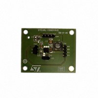
Manufacturer Part Number
STEVAL-ISA044V2
Description
BOARD EVAL BASED ON ST1S10
Manufacturer
STMicroelectronics
Type
DC/DC Switching Converters, Regulators & Controllersr
Specifications of STEVAL-ISA044V2
Mfg Application Notes
ST1S10 AppNote
Main Purpose
DC/DC, Step Down
Outputs And Type
1, Non-Isolated
Current - Output
3A
Voltage - Input
2.5 ~ 18V
Regulator Topology
Buck
Frequency - Switching
900kHz
Board Type
Fully Populated
Utilized Ic / Part
ST1S10
Input Voltage
2.5 V to 18 V
Product
Power Management Modules
Silicon Manufacturer
ST Micro
Silicon Core Number
ST1S10
Kit Application Type
Power Management - Voltage Regulator
Rohs Compliant
Yes
Lead Free Status / RoHS Status
Lead free / RoHS Compliant
Voltage - Output
-
Power - Output
-
Lead Free Status / Rohs Status
Lead free / RoHS Compliant
For Use With/related Products
ST1S10
Other names
497-8229
STEVAL-ISA044V2
STEVAL-ISA044V2


Application information
5.4
5.5
10/26
reduce ripple voltages due to the parasitic inductive effect, the output capacitor connection
paths should be kept as short as possible.
The ST1S10 has been designed to perform best with ceramic capacitors. Under typical
application conditions a minimum ceramic capacitor value of 22 µF is recommended on the
output, but higher values are suitable considering that the control loop has been designed to
work properly with a natural output LC frequency provided by a 3.3 µH inductor and 22 µF
output capacitor. If the high capacitive load application circuit shown in
47 µF (or 2 x 22 µF capacitors in parallel) could be needed as described in the OCP and
SCP operation
The use of ceramic capacitors with voltage ratings in the range of 1.5 times the maximum
output voltage is recommended.
Output capacitor (0.8 V < V
For applications with lower output voltage levels (V
inductor values should be selected in a way that improves the DC-DC control loop behavior.
In this output condition two cases must be considered: V
For V
shown in
For V
the 2 x 22 µF output capacitors as shown in
Output voltage selection
The output voltage can be adjusted from 0.8 V up to 85% of the input voltage level by
connecting a resistor divider (see R1 and R2 in the typical application circuit) between the
output and the V
compromise in terms of current consumption. Once the R2 value is selected, R1 can be
calculated using the following equation:
Equation 6
R1 = R2 x (V
where V
Lower values are suitable as well, but will increase current consumption. Be aware that duty
cycle must be kept below 85% at all application conditions, so that:
Equation 7
D = (V
where V
drop across the internal PDMOS.
Note that once the output current is fixed, higher V
of the device leading to an increase in the operating junction temperature. It is
recommended to select a V
thermal shut-down protection threshold (150°C typ.) at the rated output current. The
following equation can be used to calculate the junction temperature (T
IN
IN
OUT
> 8 V, a 100 µF electrolytic capacitor with ESR < 0.1
< 8 V the use of 2 x 22 µF capacitors in parallel to the output is recommended, as
FB
F
Figure
is the voltage drop across the internal NMOS, and V
+ V
= 0.8 V (typ.).
OUT
F
Section
) / (V
4.
FB
- V
pin. A resistor divider with R2 in the range of 20 k
FB
IN
-V
) / V
5.8.5. of this document.
SW
FB
) < 0.85
OUT
Doc ID 13844 Rev 4
level which maintains the junction temperature below the
OUT
Figure
< 2.5 V)
OUT
OUT
5.
levels increase the power dissipation
< 2.5 V) the output capacitance and
IN
> 8 V and V
Ω
should be added in parallel to
SW
represents the voltage
Ω
IN
Figure 3
J
is a suitable
):
< 8 V.
is used, a
ST1S10
Related parts for STEVAL-ISA044V2
Image
Part Number
Description
Manufacturer
Datasheet
Request
R

Part Number:
Description:
BOARD RGB CTR ST7,STP08C596MTR
Manufacturer:
STMicroelectronics
Datasheet:

Part Number:
Description:
Power Management IC Development Tools Full Speed USB to RS232 Bridge Demo
Manufacturer:
STMicroelectronics
Datasheet:
Part Number:
Description:
Power Management IC Development Tools 2.5W solar eval BRD USB SPV1040 LD39050
Manufacturer:
STMicroelectronics
Datasheet:

Part Number:
Description:
BOARD EVAL FOR MEMS SENSORS
Manufacturer:
STMicroelectronics
Datasheet:

Part Number:
Description:
KIT DEV STARTER ST10F276Z5
Manufacturer:
STMicroelectronics
Datasheet:

Part Number:
Description:
BOARD EVAL HDMI $ VIDEO SWITCH
Manufacturer:
STMicroelectronics
Datasheet:

Part Number:
Description:
BOARD DEMO ACCELEROMETER DIL24
Manufacturer:
STMicroelectronics
Datasheet:

Part Number:
Description:
BOARD STLM75/STDS75/ST72F651
Manufacturer:
STMicroelectronics
Datasheet:

Part Number:
Description:
EVAL BOARD 3AXIS MEMS ACCELLRMTR
Manufacturer:
STMicroelectronics
Datasheet:

Part Number:
Description:
BOARD EVAL 8BIT MICRO + TDE1708
Manufacturer:
STMicroelectronics
Datasheet:
Part Number:
Description:
STMicroelectronics [RIPPLE-CARRY BINARY COUNTER/DIVIDERS]
Manufacturer:
STMicroelectronics
Datasheet:
Part Number:
Description:
STMicroelectronics [LIQUID-CRYSTAL DISPLAY DRIVERS]
Manufacturer:
STMicroelectronics
Datasheet:
Part Number:
Description:
BOARD EVAL FOR MEMS SENSORS
Manufacturer:
STMicroelectronics
Datasheet: