STEVAL-ISA044V2 STMicroelectronics, STEVAL-ISA044V2 Datasheet - Page 9
STEVAL-ISA044V2
Manufacturer Part Number
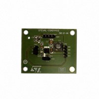
STEVAL-ISA044V2
Description
BOARD EVAL BASED ON ST1S10
Manufacturer
STMicroelectronics
Type
DC/DC Switching Converters, Regulators & Controllersr
Specifications of STEVAL-ISA044V2
Mfg Application Notes
ST1S10 AppNote
Main Purpose
DC/DC, Step Down
Outputs And Type
1, Non-Isolated
Current - Output
3A
Voltage - Input
2.5 ~ 18V
Regulator Topology
Buck
Frequency - Switching
900kHz
Board Type
Fully Populated
Utilized Ic / Part
ST1S10
Input Voltage
2.5 V to 18 V
Product
Power Management Modules
Silicon Manufacturer
ST Micro
Silicon Core Number
ST1S10
Kit Application Type
Power Management - Voltage Regulator
Rohs Compliant
Yes
Lead Free Status / RoHS Status
Lead free / RoHS Compliant
Voltage - Output
-
Power - Output
-
Lead Free Status / Rohs Status
Lead free / RoHS Compliant
For Use With/related Products
ST1S10
Other names
497-8229
STEVAL-ISA044V2
STEVAL-ISA044V2


ST1S10
5.3
Equation 2
D = (V
where V
drop across the internal PDMOS. The minimum duty cycle (at V
duty cycle (at V
through the input capacitor.
A minimum value of 4.7 µF for the V
suitable in most application conditions. A 10 µF or higher ceramic capacitor for the V
and a 1 µF or higher for the V
impedance or where long wires are needed between the power supply source and the V
pins. The above higher input capacitor values are also recommended in cases where an
output capacitive load is present (47 µF < C
switching peak current drawn from the input capacitor during the start-up transient.
In cases of very high output capacitive loads (C
values shall be modified as described in the OCP and SCP operation
document.
The input ceramic capacitors should have a voltage rating in the range of 1.5 times the
maximum input voltage and be located as close as possible to V
Output capacitor (V
The most important parameters for the output capacitor are the capacitance, the ESR and
the voltage rating. The capacitance and the ESR affect the control loop stability, the output
ripple voltage and transient response of the regulator.
The ripple due to the capacitance can be calculated with the following equation:
Equation 3
V
where F
current, which can be calculated as:
Equation 4
ΔI
where D is the duty cycle.
The ripple due to the ESR is given by:
Equation 5
V
The equations above can be used to define the capacitor selection range, but final values
should be verified by testing an evaluation circuit.
Lower ESR ceramic capacitors are usually recommended to reduce the output ripple
voltage. Capacitors with higher voltage ratings have lower ESR values, resulting in lower
output ripple voltage.
Also, the capacitor ESL value impacts the output ripple voltage, but ceramic capacitors
usually have very low ESL, making ripple voltages due to the ESL negligible. In order to
RIPPLE(C)
RIPPLE
SW
= [(V
OUT
(ESR) = ΔI
S
F
is the PWM switching frequency and ΔI
is the voltage drop across the internal NMOS, and V
IN
+ V
= (0.125 x ΔI
- V
F
) / (V
IN_min
OUT
SW
) / (F
IN
) should be considered in order to determine the max I
x ESR
- V
SW
S
SW
x L)] x D
) / (F
)
IN_A
OUT
Doc ID 13844 Rev 4
S
x C
are recommended in cases of higher power supply source
> 2.5 V)
IN_SW
OUT
)
and a 0.1 µF ceramic capacitor for the V
LOAD
LOAD
SW
< 100 µF), which could impact the
is the inductor peak-to-peak switching
> 100 µF), all input/output capacitor
SW
IN_max
IN
represents the voltage
Application information
pins.
Section 5.8.5
) and the maximum
RMS
flowing
IN_A
of this
IN_SW
are
9/26
IN
Related parts for STEVAL-ISA044V2
Image
Part Number
Description
Manufacturer
Datasheet
Request
R

Part Number:
Description:
BOARD RGB CTR ST7,STP08C596MTR
Manufacturer:
STMicroelectronics
Datasheet:

Part Number:
Description:
Power Management IC Development Tools Full Speed USB to RS232 Bridge Demo
Manufacturer:
STMicroelectronics
Datasheet:
Part Number:
Description:
Power Management IC Development Tools 2.5W solar eval BRD USB SPV1040 LD39050
Manufacturer:
STMicroelectronics
Datasheet:

Part Number:
Description:
BOARD EVAL FOR MEMS SENSORS
Manufacturer:
STMicroelectronics
Datasheet:

Part Number:
Description:
KIT DEV STARTER ST10F276Z5
Manufacturer:
STMicroelectronics
Datasheet:

Part Number:
Description:
BOARD EVAL HDMI $ VIDEO SWITCH
Manufacturer:
STMicroelectronics
Datasheet:

Part Number:
Description:
BOARD DEMO ACCELEROMETER DIL24
Manufacturer:
STMicroelectronics
Datasheet:

Part Number:
Description:
BOARD STLM75/STDS75/ST72F651
Manufacturer:
STMicroelectronics
Datasheet:

Part Number:
Description:
EVAL BOARD 3AXIS MEMS ACCELLRMTR
Manufacturer:
STMicroelectronics
Datasheet:

Part Number:
Description:
BOARD EVAL 8BIT MICRO + TDE1708
Manufacturer:
STMicroelectronics
Datasheet:
Part Number:
Description:
STMicroelectronics [RIPPLE-CARRY BINARY COUNTER/DIVIDERS]
Manufacturer:
STMicroelectronics
Datasheet:
Part Number:
Description:
STMicroelectronics [LIQUID-CRYSTAL DISPLAY DRIVERS]
Manufacturer:
STMicroelectronics
Datasheet:
Part Number:
Description:
BOARD EVAL FOR MEMS SENSORS
Manufacturer:
STMicroelectronics
Datasheet: