STEVAL-ISA044V2 STMicroelectronics, STEVAL-ISA044V2 Datasheet - Page 14
STEVAL-ISA044V2
Manufacturer Part Number
STEVAL-ISA044V2
Description
BOARD EVAL BASED ON ST1S10
Manufacturer
STMicroelectronics
Type
DC/DC Switching Converters, Regulators & Controllersr
Specifications of STEVAL-ISA044V2
Mfg Application Notes
ST1S10 AppNote
Main Purpose
DC/DC, Step Down
Outputs And Type
1, Non-Isolated
Current - Output
3A
Voltage - Input
2.5 ~ 18V
Regulator Topology
Buck
Frequency - Switching
900kHz
Board Type
Fully Populated
Utilized Ic / Part
ST1S10
Input Voltage
2.5 V to 18 V
Product
Power Management Modules
Silicon Manufacturer
ST Micro
Silicon Core Number
ST1S10
Kit Application Type
Power Management - Voltage Regulator
Rohs Compliant
Yes
Lead Free Status / RoHS Status
Lead free / RoHS Compliant
Voltage - Output
-
Power - Output
-
Lead Free Status / Rohs Status
Lead free / RoHS Compliant
For Use With/related Products
ST1S10
Other names
497-8229
STEVAL-ISA044V2
STEVAL-ISA044V2


Layout considerations
6
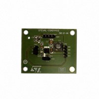
Figure 6.
14/26
Layout considerations
Layout is an important step in design for all switching power supplies.
High-speed operation (900 kHz) of the ST1S10 device demands careful attention to PCB
layout. Care must be taken in board layout to get device performance, otherwise the
regulator could show poor line and load regulation, stability issues as well as EMI problems.
It is critical to provide a low inductance, impedance ground path. Therefore, use wide and
short traces for the main current paths.
The input capacitor must be placed as close as possible to the IC pins as well as the
inductor and output capacitor. Use a common ground node for power ground and a different
one for control ground (AGND) to minimize the effects of ground noise. Connect these
ground nodes together underneath the device and make sure that small signal components
returning to the AGND pin and do not share the high current path of C
The feedback voltage sense line (V
routed away from noisy components and traces (e.g., SW line). Its trace should be
minimized and shielded by a guard-ring connected to the ground.
PCB layout suggestion
Doc ID 13844 Rev 4
FB
) should be connected right to the output capacitor and
CN1 = Input power supply
CN2 = Enable/Disable
CN3 = Input sync.
CN4 = V
Input capacitor C1 must be
placed as close as possible
to the IC pins as well as the
inductor L1 and output
capacitor C2
Via holes from thermal pad
to bottom layer
IN
OUT
and C
OUT
.
ST1S10
Related parts for STEVAL-ISA044V2
Image
Part Number
Description
Manufacturer
Datasheet
Request
R

Part Number:
Description:
BOARD RGB CTR ST7,STP08C596MTR
Manufacturer:
STMicroelectronics
Datasheet:

Part Number:
Description:
Power Management IC Development Tools Full Speed USB to RS232 Bridge Demo
Manufacturer:
STMicroelectronics
Datasheet:
Part Number:
Description:
Power Management IC Development Tools 2.5W solar eval BRD USB SPV1040 LD39050
Manufacturer:
STMicroelectronics
Datasheet:

Part Number:
Description:
BOARD EVAL FOR MEMS SENSORS
Manufacturer:
STMicroelectronics
Datasheet:

Part Number:
Description:
KIT DEV STARTER ST10F276Z5
Manufacturer:
STMicroelectronics
Datasheet:

Part Number:
Description:
BOARD EVAL HDMI $ VIDEO SWITCH
Manufacturer:
STMicroelectronics
Datasheet:

Part Number:
Description:
BOARD DEMO ACCELEROMETER DIL24
Manufacturer:
STMicroelectronics
Datasheet:

Part Number:
Description:
BOARD STLM75/STDS75/ST72F651
Manufacturer:
STMicroelectronics
Datasheet:

Part Number:
Description:
EVAL BOARD 3AXIS MEMS ACCELLRMTR
Manufacturer:
STMicroelectronics
Datasheet:

Part Number:
Description:
BOARD EVAL 8BIT MICRO + TDE1708
Manufacturer:
STMicroelectronics
Datasheet:
Part Number:
Description:
STMicroelectronics [RIPPLE-CARRY BINARY COUNTER/DIVIDERS]
Manufacturer:
STMicroelectronics
Datasheet:
Part Number:
Description:
STMicroelectronics [LIQUID-CRYSTAL DISPLAY DRIVERS]
Manufacturer:
STMicroelectronics
Datasheet:
Part Number:
Description:
BOARD EVAL FOR MEMS SENSORS
Manufacturer:
STMicroelectronics
Datasheet: