NCP5030MTTXGEVB ON Semiconductor, NCP5030MTTXGEVB Datasheet - Page 12
NCP5030MTTXGEVB
Manufacturer Part Number
NCP5030MTTXGEVB
Description
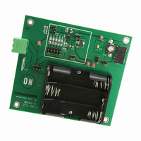
EVAL BOARD FOR NCP5030MTTXG
Manufacturer
ON Semiconductor
Datasheets
1.NCP5030MTTXG.pdf
(14 pages)
2.NCP5030MTTXGEVB.pdf
(1 pages)
3.NCP5030MTTXGEVB.pdf
(7 pages)
Specifications of NCP5030MTTXGEVB
Design Resources
NCP5030MTTXG EVB BOM NCP5030MTTXGEVB Gerber Files NCP5030MTTXG EVB Schematic
Current - Output / Channel
900mA
Outputs And Type
1, Non-Isolated
Voltage - Output
2.2 ~ 5.5 V
Features
Adjustable
Voltage - Input
2.7 ~ 5.5V
Utilized Ic / Part
NCP5030
Rohs Compliant
NO
Lead Free Status / RoHS Status
Lead free / RoHS Compliant
For Use With/related Products
NCP5030MTTXG
Other names
NCP5030MTTXGEVBOS


from the supply according to the application’s specific
requirements. The I
in a minimum resistor value of 30 kW. Please refer to
Figure 8 I
value versus I
the needs of the application, the inductor sizing can be
scaled appropriately to the specific requirements. This
allows the PCB footprint to be minimized.
Input and Output Capacitors Selection
the load current during the T
loop stability and minimize the output ripple, at least 22 mF
low ESR multi−layer ceramic capacitor type X5R is
recommended.
X5R or an equivalent low ESR ceramic capacitor. Near the
PV
is needed. Regarding V
is sufficient. Some recommended capacitors include but
are not limited to:
22 mF 6.3 V 0805
22 mF 6.3 V 1206
10 mF 6.3 V 0805
Over Voltage Protection (OVP)
open load condition such as a lost connection to the White
LED, the converter keeps supplying current to the Cout
capacitor causing the output voltage to rise rapidly. To
prevent the device from being damaged and to eliminate
external protection components such as zener diode, the
NCP5030 incorporates an OVP circuit, which monitors the
output voltage with a resistive divider network and a
comparator and voltage reference. If the output reaches 6 V
(nominal), the OVP circuit will detect a fault and inhibit
PWM operation. This comparator has 200 mV hysteresis to
allow the PWM operation to resume automatically when
the load is reconnected and when the voltage drops below
5.8 V.
C
The V
TDK: C2012X5R0J226MTJ
MURATA: GRM31CR60J226KE19L
TDK C2012X5R0J106MT
The NCP5030 regulates the load current. If there is an
IN
OUT
pin at least 10 mF 6.3 V or higher ceramic capacitor
stores energy during the T
IN
PEAK_MAX
and PV
PEAK_MAX
IN
peak
input pin need to be bypassed by a
Vs R
IN
maximum value is 4 A, resulting
. By limiting the peak current to
pin a 1 mF 6.3 V close to the pad
PCA
ON
phase. In order ensure the
page 6 to choose R
OFF
phase and sustains
http://onsemi.com
PCA
12
Under Voltage Lock Out
conditions, the device has a built−in Under−Voltage Lock
Out (UVLO) circuit. The device remains disabled until the
input voltage exceeds 2.35 V (nominal). This circuit has
100 mV hysteresis to provide noise immunity to transient
conditions.
Thermal Protection
the device if the junction temperature exceeds 160°C.
When the junction temperature drops below 140°C, normal
operation will resume.
Layout Recommendations
observed to the PCB board layout and component
placement. To prevent electromagnetic interference (EMI)
problems and reduce voltage ripple of the device any
copper trace, which see high frequency switching path,
should be optimized. So the input and output bypass
ceramic capacitor, C
must be placed as close as possible the NCP5030 and
connected directly between pins and ground plane. In
additional, the track connection between the inductor and
the switching input, SW pin must be minimized to reduce
EMI radiation.
To ensure proper operation under low input voltage
Normal operation of the NCP5030 is disabled to protect
As with all switching DC/DC converter, care must be
Figure 24. Recommended PCB Layout
IN
and C
TBD
OUT
as depicted in Figure 24
Related parts for NCP5030MTTXGEVB
Image
Part Number
Description
Manufacturer
Datasheet
Request
R

Part Number:
Description:
ON Semiconductor [VOLTAGE REGULATOR]
Manufacturer:
ON Semiconductor
Datasheet:
Part Number:
Description:
357-036-542-201 CARDEDGE 36POS DL .156 BLK LOPRO
Manufacturer:
ON Semiconductor
Datasheet:
Part Number:
Description:
357-036-542-201 CARDEDGE 36POS DL .156 BLK LOPRO
Manufacturer:
ON Semiconductor
Datasheet:
Part Number:
Description:
357-036-542-201 CARDEDGE 36POS DL .156 BLK LOPRO
Manufacturer:
ON Semiconductor
Datasheet:
Part Number:
Description:
357-036-542-201 CARDEDGE 36POS DL .156 BLK LOPRO
Manufacturer:
ON Semiconductor
Datasheet:
Part Number:
Description:
357-036-542-201 CARDEDGE 36POS DL .156 BLK LOPRO
Manufacturer:
ON Semiconductor
Datasheet:
Part Number:
Description:
357-036-542-201 CARDEDGE 36POS DL .156 BLK LOPRO
Manufacturer:
ON Semiconductor
Datasheet:
Part Number:
Description:
357-036-542-201 CARDEDGE 36POS DL .156 BLK LOPRO
Manufacturer:
ON Semiconductor
Datasheet:
Part Number:
Description:
357-036-542-201 CARDEDGE 36POS DL .156 BLK LOPRO
Manufacturer:
ON Semiconductor
Datasheet:
Part Number:
Description:
357-036-542-201 CARDEDGE 36POS DL .156 BLK LOPRO
Manufacturer:
ON Semiconductor
Datasheet:
Part Number:
Description:
357-036-542-201 CARDEDGE 36POS DL .156 BLK LOPRO
Manufacturer:
ON Semiconductor
Datasheet:
Part Number:
Description:
Manufacturer:
ON Semiconductor
Datasheet:
Part Number:
Description:
Manufacturer:
ON Semiconductor
Datasheet:
Part Number:
Description:
Manufacturer:
ON Semiconductor
Datasheet: