NCP5030MTTXGEVB ON Semiconductor, NCP5030MTTXGEVB Datasheet - Page 5
NCP5030MTTXGEVB
Manufacturer Part Number
NCP5030MTTXGEVB
Description
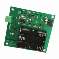
EVAL BOARD FOR NCP5030MTTXG
Manufacturer
ON Semiconductor
Datasheets
1.NCP5030MTTXG.pdf
(14 pages)
2.NCP5030MTTXGEVB.pdf
(1 pages)
3.NCP5030MTTXGEVB.pdf
(7 pages)
Specifications of NCP5030MTTXGEVB
Design Resources
NCP5030MTTXG EVB BOM NCP5030MTTXGEVB Gerber Files NCP5030MTTXG EVB Schematic
Current - Output / Channel
900mA
Outputs And Type
1, Non-Isolated
Voltage - Output
2.2 ~ 5.5 V
Features
Adjustable
Voltage - Input
2.7 ~ 5.5V
Utilized Ic / Part
NCP5030
Rohs Compliant
NO
Lead Free Status / RoHS Status
Lead free / RoHS Compliant
For Use With/related Products
NCP5030MTTXG
Other names
NCP5030MTTXGEVBOS


8. T
9. Efficiency is defined by 100 * (P
10. L = 4.7 mH (TDK RLF7030T−4R7M3R4), C
11. Guaranteed by design and characterized.
12. The overall tolerance is dependent on the accuracy of the external resistor.
ELECTRICAL CHARACTERISTICS
Operational Power Supply
Maximum Inductor Current (Note 11) (See Figure 8)
Switches P1 and P2 ON Resistance
Switches N1 and N2 ON Resistance
Switches P1 and P2 Leakage Current
Switches N1 and N2 Leakage Current
Internal Oscillator Frequency (Note 8)
Efficiency (Notes 9, 10 and 11)
Output Voltage Range (Note 11)
V
V
Threshold to Change Mode Hysteresis
Available Output Power (Note 11)
Feedback Voltage Threshold in Steady State at 25°C
Line Regulation, Measured on FB Pin (Note 8)
Feedback Input Current
Standby Current at I
Quiescent Current Switching at I
V
Undervoltage Lockout Hysteresis
Soft−start Time (Note 11)
Limit of CTRL pin PWM Dimming Frequency (Note 11)
Thermal Shutdown Protection
Thermal Shutdown Protection Hysteresis
Voltage Input Logic Low
Voltage Input Logic High
CTRL Pin Pulldown Resistance
When V
From DC to 100 Hz and R
(Note 12)
Threshold to Enable the Converter
OUT
IN
IN
A
−V
Undervoltage Lockout
between −10°C to +85°C
−V
OUT
IN
in
Threshold to Change Mode from Boost to Buck−Boost
Threshold to Change Mode from Buck−Boost to Buck
≥ 3.1 V (V
OUT
out
= 4.7 V, 900 mA)
= 0 mA, CTRL = Low, V
FB
Characteristic
= 1 W
OUT
out
/P
= 0 mA, CTRL = High, V
in
) at 25°C. V
(
Limits apply for T
out
= 22 mF X5R
bat
in
= 4.2 V
= 3.3 V, I
http://onsemi.com
A
between −40°C to +85°C and V
bat
OUT
= 4.2 V
= 500 mA, Load = 1 LED (V
5
N
P
I
MOS
MOS
PEAK_MAX
Symbol
P
N
T
H
U
T
R
F
F
V
P
U
T
BOOST
MOS
F
MOS
MODE
F
F
I
S
T
E
BUCK
V
BVLR
I
VLOH
V
STB
V
CTRL
OSC
SDH
OUT
OUT
QS
VLO
DIM
BV
BC
ST
SD
R
FF
IN
R
IH
IL
DSON
DSON
L
L
in
f
= 3.6 V unless otherwise noted.)
= 3.9 V)
−20%
Min
600
190
150
2.7
2.2
4.3
2.2
1.2
−
−
−
−
−
−
−
−
−
−
−
−
−
−
−
−
−
−
1000
Typ
100
100
700
375
650
100
200
100
160
220
4.0
0.5
0.5
5.0
0.3
5.0
2.4
0.2
85
20
−
−
−
−
−
−
+20%
Max
800
210
290
5.5
5.5
0.1
3.0
2.6
0.4
−
−
−
−
−
−
−
−
−
−
−
−
−
−
−
−
−
mV/V
Unit
kHz
kHz
mW
mW
mV
mV
mV
mV
mA
mV
mA
mA
mA
mA
kW
°C
°C
W
ms
%
V
A
V
V
V
V
Related parts for NCP5030MTTXGEVB
Image
Part Number
Description
Manufacturer
Datasheet
Request
R

Part Number:
Description:
ON Semiconductor [VOLTAGE REGULATOR]
Manufacturer:
ON Semiconductor
Datasheet:
Part Number:
Description:
357-036-542-201 CARDEDGE 36POS DL .156 BLK LOPRO
Manufacturer:
ON Semiconductor
Datasheet:
Part Number:
Description:
357-036-542-201 CARDEDGE 36POS DL .156 BLK LOPRO
Manufacturer:
ON Semiconductor
Datasheet:
Part Number:
Description:
357-036-542-201 CARDEDGE 36POS DL .156 BLK LOPRO
Manufacturer:
ON Semiconductor
Datasheet:
Part Number:
Description:
357-036-542-201 CARDEDGE 36POS DL .156 BLK LOPRO
Manufacturer:
ON Semiconductor
Datasheet:
Part Number:
Description:
357-036-542-201 CARDEDGE 36POS DL .156 BLK LOPRO
Manufacturer:
ON Semiconductor
Datasheet:
Part Number:
Description:
357-036-542-201 CARDEDGE 36POS DL .156 BLK LOPRO
Manufacturer:
ON Semiconductor
Datasheet:
Part Number:
Description:
357-036-542-201 CARDEDGE 36POS DL .156 BLK LOPRO
Manufacturer:
ON Semiconductor
Datasheet:
Part Number:
Description:
357-036-542-201 CARDEDGE 36POS DL .156 BLK LOPRO
Manufacturer:
ON Semiconductor
Datasheet:
Part Number:
Description:
357-036-542-201 CARDEDGE 36POS DL .156 BLK LOPRO
Manufacturer:
ON Semiconductor
Datasheet:
Part Number:
Description:
357-036-542-201 CARDEDGE 36POS DL .156 BLK LOPRO
Manufacturer:
ON Semiconductor
Datasheet:
Part Number:
Description:
Manufacturer:
ON Semiconductor
Datasheet:
Part Number:
Description:
Manufacturer:
ON Semiconductor
Datasheet:
Part Number:
Description:
Manufacturer:
ON Semiconductor
Datasheet: