NCP5030MTTXGEVB ON Semiconductor, NCP5030MTTXGEVB Datasheet - Page 7
NCP5030MTTXGEVB
Manufacturer Part Number
NCP5030MTTXGEVB
Description
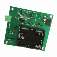
EVAL BOARD FOR NCP5030MTTXG
Manufacturer
ON Semiconductor
Datasheets
1.NCP5030MTTXG.pdf
(14 pages)
2.NCP5030MTTXGEVB.pdf
(1 pages)
3.NCP5030MTTXGEVB.pdf
(7 pages)
Specifications of NCP5030MTTXGEVB
Design Resources
NCP5030MTTXG EVB BOM NCP5030MTTXGEVB Gerber Files NCP5030MTTXG EVB Schematic
Current - Output / Channel
900mA
Outputs And Type
1, Non-Isolated
Voltage - Output
2.2 ~ 5.5 V
Features
Adjustable
Voltage - Input
2.7 ~ 5.5V
Utilized Ic / Part
NCP5030
Rohs Compliant
NO
Lead Free Status / RoHS Status
Lead free / RoHS Compliant
For Use With/related Products
NCP5030MTTXG
Other names
NCP5030MTTXGEVBOS


150
100
730
720
710
700
690
680
670
660
650
640
630
620
610
600
50
−50
−40
Figure 11. Transitional Period Switch Pins (LX1
and LX2) from Boost to Buck−Boost when
Figure 9. NMOS R
−20
−25
Temperature V
Figure 13. Oscillator Frequency vs.
V
V
in
OUT
= 3.1 V
0
0
TEMPERATURE (°C)
TEMPERATURE (°C)
− V
V
in
IN
= 3.6 V
20
25
OUT
is < than 375 mV
DSON
= 3.6 V, V
TYPICAL PERFORMANCE CHARACTERISTICS
50
40
vs. Temperature
IN
60
75
= 3.6 V
V
V
in
in
= 2.7 V
100
= 4.2 V
80
http://onsemi.com
125
100
7
150
100
210
205
200
195
190
50
−40
−40
Figure 12. Transitional Period Switch Pins (LX1
Figure 14. Feedback Voltage vs. Temperature
and LX2) from Buck to Buck−Boost when
Figure 10. PMOS R
−20
−20
V
V
in
IN
= 3.1 V
V
0
0
OUT
− V
TEMPERATURE (°C)
TEMPERATURE (°C)
V
OUT
in
= 3.6 V, V
20
= 3.6 V
20
is > than 650 mV
DSON
40
40
IN
vs. Temperature
= 3.6 V
60
60
V
V
in
in
80
= 2.7 V
= 4.2 V
80
100
100
Related parts for NCP5030MTTXGEVB
Image
Part Number
Description
Manufacturer
Datasheet
Request
R

Part Number:
Description:
ON Semiconductor [VOLTAGE REGULATOR]
Manufacturer:
ON Semiconductor
Datasheet:
Part Number:
Description:
357-036-542-201 CARDEDGE 36POS DL .156 BLK LOPRO
Manufacturer:
ON Semiconductor
Datasheet:
Part Number:
Description:
357-036-542-201 CARDEDGE 36POS DL .156 BLK LOPRO
Manufacturer:
ON Semiconductor
Datasheet:
Part Number:
Description:
357-036-542-201 CARDEDGE 36POS DL .156 BLK LOPRO
Manufacturer:
ON Semiconductor
Datasheet:
Part Number:
Description:
357-036-542-201 CARDEDGE 36POS DL .156 BLK LOPRO
Manufacturer:
ON Semiconductor
Datasheet:
Part Number:
Description:
357-036-542-201 CARDEDGE 36POS DL .156 BLK LOPRO
Manufacturer:
ON Semiconductor
Datasheet:
Part Number:
Description:
357-036-542-201 CARDEDGE 36POS DL .156 BLK LOPRO
Manufacturer:
ON Semiconductor
Datasheet:
Part Number:
Description:
357-036-542-201 CARDEDGE 36POS DL .156 BLK LOPRO
Manufacturer:
ON Semiconductor
Datasheet:
Part Number:
Description:
357-036-542-201 CARDEDGE 36POS DL .156 BLK LOPRO
Manufacturer:
ON Semiconductor
Datasheet:
Part Number:
Description:
357-036-542-201 CARDEDGE 36POS DL .156 BLK LOPRO
Manufacturer:
ON Semiconductor
Datasheet:
Part Number:
Description:
357-036-542-201 CARDEDGE 36POS DL .156 BLK LOPRO
Manufacturer:
ON Semiconductor
Datasheet:
Part Number:
Description:
Manufacturer:
ON Semiconductor
Datasheet:
Part Number:
Description:
Manufacturer:
ON Semiconductor
Datasheet:
Part Number:
Description:
Manufacturer:
ON Semiconductor
Datasheet: