ADP1720-3.3-EVALZ Analog Devices Inc, ADP1720-3.3-EVALZ Datasheet - Page 10
ADP1720-3.3-EVALZ
Manufacturer Part Number
ADP1720-3.3-EVALZ
Description
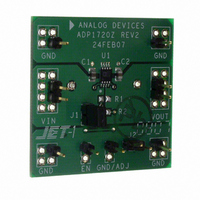
BOARD EVAL FOR ADP1720-3.3
Manufacturer
Analog Devices Inc
Datasheet
1.ADP1720-3.3-EVALZ.pdf
(16 pages)
Specifications of ADP1720-3.3-EVALZ
Design Resources
4 mA-to-20 mA Loop-Powered Temperature Monitor Using ADuC7060/1 (CN0145)
Channels Per Ic
1 - Single
Voltage - Output
3.3V
Current - Output
50mA
Voltage - Input
4 ~ 28V
Regulator Type
Positive Fixed
Operating Temperature
-40°C ~ 125°C
Board Type
Fully Populated
Utilized Ic / Part
ADP1720
Lead Free Status / RoHS Status
Lead free / RoHS Compliant


ADP1720
THEORY OF OPERATION
The ADP1720 is a low dropout, BiCDMOS linear regulator that
operates from a 4 V to 28 V input rail and provides up to 50 mA
of output current. Ground current in shutdown mode is typically
700 nA. The ADP1720 is stable and provides high power supply
rejection ratio (PSRR) and excellent line and load transient
response with just a small 1 μF ceramic output capacitor.
Internally, the ADP1720 consists of a reference, an error ampli-
fier, a feedback voltage divider, and a DMOS pass transistor.
Output current is delivered via the DMOS pass device, which is
controlled by the error amplifier. The error amplifier compares
the reference voltage with the feedback voltage from the output
and amplifies the difference. If the feedback voltage is lower than
the reference voltage, the gate of the DMOS device is pulled
lower, allowing more current to pass and increasing the output
voltage. If the feedback voltage is higher than the reference
voltage, the gate of the PNP device is pulled higher, allowing
less current to pass and decreasing the output voltage.
The ADP1720 is available in two versions, one with fixed output
voltage options (see Figure 1) and one with an adjustable output
voltage (see Figure 2). The fixed output voltage options are set
internally to either 5.0 V or 3.3 V, using an internal feedback
network. The adjustable output voltage can be set to between
1.225 V and 5.0 V by an external voltage divider connected from
OUT to ADJ. The ADP1720 uses the EN pin to enable and
disable the OUT pin under normal operating conditions. When
EN is high, OUT turns on; when EN is low, OUT turns off. For
automatic startup, EN can be tied to IN.
EN
IN
THERMAL PROTECT
SHUTDOWN
CURRENT LIMIT
REFERENCE
Figure 19. Internal Block Diagram
GND
OUT
GND/ADJ
Rev. A | Page 10 of 16
ADJUSTABLE OUTPUT VOLTAGE
(ADP1720 ADJUSTABLE)
The ADP1720 adjustable version can have its output voltage
set over a 1.225 V to 5.0 V range. The output voltage is set by
connecting a resistive voltage divider from OUT to ADJ. The
output voltage is calculated using the equation
where:
R1 is the resistor from OUT to ADJ.
R2 is the resistor from ADJ to GND.
To make calculation of R1 and R2 easier, Equation 1 can be
rearranged as follows:
The maximum bias current into ADJ is 100 nA; therefore,
when less than 0.5% error is due to the bias current, use values
less than 60 kΩ for R2.
V
R1 = R2 [(V
OUT
= 1.225 V (1 + R1/R2)
OUT
/1.225) – 1]
(1)
(2)
Related parts for ADP1720-3.3-EVALZ
Image
Part Number
Description
Manufacturer
Datasheet
Request
R

Part Number:
Description:
50 mA, High Voltage, Micropower Linear Regulator
Manufacturer:
Analog Devices
Datasheet:

Part Number:
Description:
BOARD EVAL FOR ADP1720-5
Manufacturer:
Analog Devices Inc
Datasheet:

Part Number:
Description:
BOARD EVAL FOR ADP1720-ADJ
Manufacturer:
Analog Devices Inc
Datasheet:

Part Number:
Description:
Blank ADISimPower Eval ADP1720
Manufacturer:
Analog Devices Inc
Datasheet:
Part Number:
Description:
50mA High-Voltage Micro-power LDO in MSOP
Manufacturer:
Analog Devices
Datasheet:
Part Number:
Description:
50mA High-Voltage Micro-power LDO in MSOP
Manufacturer:
Analog Devices
Datasheet:
Part Number:
Description:
50mA High-Voltage Micro-power LDO in MSOP
Manufacturer:
Analog Devices
Datasheet:

Part Number:
Description:
±1.7g Dual-Axis IMEMS Accelerometer Evaluation Board
Manufacturer:
Analog Devices Inc
Datasheet:
Part Number:
Description:
Inertial Sensor Evaluation System
Manufacturer:
Analog Devices Inc
Datasheet:
Part Number:
Description:
Manufacturer:
Analog Devices Inc
Datasheet:
Part Number:
Description:
Manufacturer:
Analog Devices Inc
Datasheet:
Part Number:
Description:
Manufacturer:
Analog Devices Inc
Datasheet:
Part Number:
Description:
Manufacturer:
Analog Devices Inc
Datasheet: