ADP1720-3.3-EVALZ Analog Devices Inc, ADP1720-3.3-EVALZ Datasheet - Page 12
ADP1720-3.3-EVALZ
Manufacturer Part Number
ADP1720-3.3-EVALZ
Description
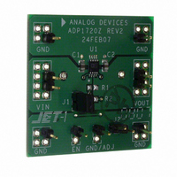
BOARD EVAL FOR ADP1720-3.3
Manufacturer
Analog Devices Inc
Datasheet
1.ADP1720-3.3-EVALZ.pdf
(16 pages)
Specifications of ADP1720-3.3-EVALZ
Design Resources
4 mA-to-20 mA Loop-Powered Temperature Monitor Using ADuC7060/1 (CN0145)
Channels Per Ic
1 - Single
Voltage - Output
3.3V
Current - Output
50mA
Voltage - Input
4 ~ 28V
Regulator Type
Positive Fixed
Operating Temperature
-40°C ~ 125°C
Board Type
Fully Populated
Utilized Ic / Part
ADP1720
Lead Free Status / RoHS Status
Lead free / RoHS Compliant


ADP1720
THERMAL CONSIDERATIONS
To guarantee reliable operation, the junction temperature of the
ADP1720 must not exceed 125°C. To ensure the junction tem-
perature stays below this maximum value, the user needs to be
aware of the parameters that contribute to junction temperature
changes. These parameters include ambient temperature, power
dissipation in the power device, and thermal resistances between
the junction and ambient air (θ
on the package assembly compounds used and the amount of
copper to which the GND pins of the package are soldered on the
PCB. Table 5 shows typical θ
for various PCB copper sizes.
Table 5.
Copper Size (mm
0
50
100
300
500
1
The junction temperature of the ADP1720 can be calculated
from the following equation:
where:
T
P
where:
I
I
V
Power dissipation due to ground current is quite small and
can be ignored. Therefore, the junction temperature equation
simplifies to the following:
As shown in Equation 5, for a given ambient temperature,
input-to-output voltage differential, and continuous load
current, there exists a minimum copper size requirement for
the PCB to ensure that the junction temperature does not rise
above 125°C. Figure 22 to Figure 27 show junction temperature
calculations for different ambient temperatures, load currents,
V
LOAD
GND
Device soldered to minimum size pin traces.
1
D
A
IN
IN
is the power dissipation in the die, given by
is the ambient temperature.
and V
to V
is the ground current.
T
P
T
is the load current.
J
D
J
= T
= T
= [(V
OUT
OUT
A
A
differentials, and areas of PCB copper.
+ (P
+ {[(V
IN
are input and output voltages, respectively.
– V
D
2
× θ
)
IN
OUT
– V
JA
) × I
)
OUT
LOAD
) × I
JA
values of the 8-lead MSOP package
] + (V
JA
LOAD
). The θ
] × θ
IN
× I
JA
JA
GND
number is dependent
}
θ
118
99
77
75
74
JA
)
(°C/W)
Rev. A | Page 12 of 16
(3)
(4)
(5)
140
120
100
140
120
100
140
120
100
80
60
40
20
80
60
40
20
80
60
40
20
0
0
0
0
0
0
MAX T
MAX T
MAX T
Figure 22. 300 mm
Figure 23. 100 mm
Figure 24. 0 mm
1mA
5mA
1mA
5mA
1mA
5mA
4
4
4
J
J
J
(DO NOT OPERATE ABOVE THIS POINT)
(DO NOT OPERATE ABOVE THIS POINT)
(DO NOT OPERATE ABOVE THIS POINT)
8
8
8
10mA
20mA
10mA
20mA
10mA
20mA
2
2
2
of PCB Copper, T
V
V
V
12
IN
of PCB Copper, T
12
IN
of PCB Copper, T
12
IN
– V
– V
– V
OUT
OUT
OUT
30mA
40mA
30mA
40mA
30mA
40mA
16
16
16
(V)
(V)
(V)
(LOAD CURRENT)
(LOAD CURRENT)
(LOAD CURRENT)
A
20
A
20
A
20
= 25°C
= 25°C
= 25°C
50mA
50mA
50mA
24
24
24
28
2
2
8
8
Related parts for ADP1720-3.3-EVALZ
Image
Part Number
Description
Manufacturer
Datasheet
Request
R

Part Number:
Description:
50 mA, High Voltage, Micropower Linear Regulator
Manufacturer:
Analog Devices
Datasheet:

Part Number:
Description:
BOARD EVAL FOR ADP1720-5
Manufacturer:
Analog Devices Inc
Datasheet:

Part Number:
Description:
BOARD EVAL FOR ADP1720-ADJ
Manufacturer:
Analog Devices Inc
Datasheet:

Part Number:
Description:
Blank ADISimPower Eval ADP1720
Manufacturer:
Analog Devices Inc
Datasheet:
Part Number:
Description:
50mA High-Voltage Micro-power LDO in MSOP
Manufacturer:
Analog Devices
Datasheet:
Part Number:
Description:
50mA High-Voltage Micro-power LDO in MSOP
Manufacturer:
Analog Devices
Datasheet:
Part Number:
Description:
50mA High-Voltage Micro-power LDO in MSOP
Manufacturer:
Analog Devices
Datasheet:

Part Number:
Description:
±1.7g Dual-Axis IMEMS Accelerometer Evaluation Board
Manufacturer:
Analog Devices Inc
Datasheet:
Part Number:
Description:
Inertial Sensor Evaluation System
Manufacturer:
Analog Devices Inc
Datasheet:
Part Number:
Description:
Manufacturer:
Analog Devices Inc
Datasheet:
Part Number:
Description:
Manufacturer:
Analog Devices Inc
Datasheet:
Part Number:
Description:
Manufacturer:
Analog Devices Inc
Datasheet:
Part Number:
Description:
Manufacturer:
Analog Devices Inc
Datasheet: