ADP1720-3.3-EVALZ Analog Devices Inc, ADP1720-3.3-EVALZ Datasheet - Page 11
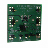
ADP1720-3.3-EVALZ
Manufacturer Part Number
ADP1720-3.3-EVALZ
Description
BOARD EVAL FOR ADP1720-3.3
Manufacturer
Analog Devices Inc
Datasheet
1.ADP1720-3.3-EVALZ.pdf
(16 pages)
Specifications of ADP1720-3.3-EVALZ
Design Resources
4 mA-to-20 mA Loop-Powered Temperature Monitor Using ADuC7060/1 (CN0145)
Channels Per Ic
1 - Single
Voltage - Output
3.3V
Current - Output
50mA
Voltage - Input
4 ~ 28V
Regulator Type
Positive Fixed
Operating Temperature
-40°C ~ 125°C
Board Type
Fully Populated
Utilized Ic / Part
ADP1720
Lead Free Status / RoHS Status
Lead free / RoHS Compliant


APPLICATIONS INFORMATION
CAPACITOR SELECTION
Output Capacitor
The ADP1720 is designed for operation with small, space-saving
ceramic capacitors, but it functionswith most commonly used
capacitors as long as care is taken about the effective series
resistance (ESR) value. The ESR of the output capacitor affects
stability of the LDO control loop. A minimum of 1 μF capacitance
with an ESR of 500 mΩ or less is recommended to ensure sta-
bility of the ADP1720. Transient response to changes in load
current is also affected by output capacitance. Using a larger
value of output capacitance improves the transient response of
the ADP1720 to large changes in load current. Figure 20 and
Figure 21 show the transient responses for output capacitance
values of 1 μF and 10 μF, respectively.
Input Bypass Capacitor
Connecting a 1 μF capacitor from IN to GND reduces the cir-
cuit sensitivity to printed circuit board (PCB) layout, especially
when encountering long input traces or high source impedance.
If greater than 1 μF of output capacitance is required, it is
recommended that the input capacitor be increased to match it.
1
1
V
V
C
C
LOAD STEP FROM 2.5mA TO 47.5mA
V
V
C
C
LOAD STEP FROM 2.5mA TO 47.5mA
IN
OUT
IN
OUT
IN
OUT
IN
OUT
Figure 21. Output Transient Response, 10 μF
= 12V
= 1µF
= 12V
= 10µF
Figure 20. Output Transient Response, 1 μF
= 1.6V
= 1.6V
= 1µF
= 10µF
TIME (2µs/DIV)
TIME (2µs/DIV)
Rev. A | Page 11 of 16
Input and Output Capacitor Properties
Any good quality ceramic capacitors can be used with the
ADP1720, as long as they meet the minimum capacitance and
maximum ESR requirements. Ceramic capacitors are manufac-
tured with a variety of dielectrics, each with different behavior
over temperature and applied voltage. Capacitors must have a
dielectric adequate to ensure the minimum capacitance over
the necessary temperature range and dc bias conditions. X5R
or X7R dielectrics with a voltage rating of 6.3 V or 10 V are
recommended for the output capacitor. X5R or X7R dielectrics
with a voltage rating of 50 V or higher are recommended for the
input capacitor.
Y5V and Z5U dielectrics are not recommended, due to their
poor temperature and dc bias characteristics.
CURRENT LIMIT AND THERMAL OVERLOAD
PROTECTION
Current limit and thermal overload protection circuits on the
ADP1720 protect the part from damage caused by excessive power
dissipation. The ADP1720 is designed to current limit when
the output load reaches 90 mA (typical). When the output
load exceeds 90 mA, the output voltage is reduced to maintain
a constant current limit.
Thermal overload protection is included, which limits the junction
temperature to a maximum of 150°C (typical). Under extreme
conditions (that is, high ambient temperature and power dissipa-
tion), when the junction temperature starts to rise above 150°C,
the output is turned off, reducing the output current to zero.
When the junction temperature drops below 135°C, the output is
turned on again, and output current is restored to its nominal value.
Consider the case where a hard short from OUT to GND occurs.
At first, the ADP1720 current limits so that only 90 mA is
conducted into the short. If self-heating of the junction is
great enough to cause its temperature to rise above 150°C,
thermal shutdown activates, turning off the output and
reducing the output current to zero. As the junction
temperature cools and drops below 135°C, the output turns on
and conducts 90 mA into the short, again causing the junction
temperature to rise above 150°C. This thermal oscillation
between 135°C and 150°C causes a current oscillation between
90 mA and 0 mA, which continues as long as the short
remains at the output.
Current and thermal limit protections are intended to protect
the device against accidental overload conditions. For reliable
operation, device power dissipation must be externally limited
so that junction temperatures do not exceed 125°C.
ADP1720
Related parts for ADP1720-3.3-EVALZ
Image
Part Number
Description
Manufacturer
Datasheet
Request
R

Part Number:
Description:
50 mA, High Voltage, Micropower Linear Regulator
Manufacturer:
Analog Devices
Datasheet:

Part Number:
Description:
BOARD EVAL FOR ADP1720-5
Manufacturer:
Analog Devices Inc
Datasheet:

Part Number:
Description:
BOARD EVAL FOR ADP1720-ADJ
Manufacturer:
Analog Devices Inc
Datasheet:

Part Number:
Description:
Blank ADISimPower Eval ADP1720
Manufacturer:
Analog Devices Inc
Datasheet:
Part Number:
Description:
50mA High-Voltage Micro-power LDO in MSOP
Manufacturer:
Analog Devices
Datasheet:
Part Number:
Description:
50mA High-Voltage Micro-power LDO in MSOP
Manufacturer:
Analog Devices
Datasheet:
Part Number:
Description:
50mA High-Voltage Micro-power LDO in MSOP
Manufacturer:
Analog Devices
Datasheet:

Part Number:
Description:
±1.7g Dual-Axis IMEMS Accelerometer Evaluation Board
Manufacturer:
Analog Devices Inc
Datasheet:
Part Number:
Description:
Inertial Sensor Evaluation System
Manufacturer:
Analog Devices Inc
Datasheet:
Part Number:
Description:
Manufacturer:
Analog Devices Inc
Datasheet:
Part Number:
Description:
Manufacturer:
Analog Devices Inc
Datasheet:
Part Number:
Description:
Manufacturer:
Analog Devices Inc
Datasheet:
Part Number:
Description:
Manufacturer:
Analog Devices Inc
Datasheet: