AD8432-EVALZ Analog Devices Inc, AD8432-EVALZ Datasheet
AD8432-EVALZ
Specifications of AD8432-EVALZ


Related parts for AD8432-EVALZ


AD8432-EVALZ Summary of contents
Page 1
... I/Q demodulator signals. The AD8432 operates on a single supply mA available × 4 mm, 24-lead LFSCP. The LFCSP features an exposed paddle that provides a low thermal resistance path to the PCB, which enables more efficient heat transfer and increases reliability. The operating temperature range is − ...
Page 2
... AD8432 TABLE OF CONTENTS Features .............................................................................................. 1 Applications ....................................................................................... 1 Functional Block Diagram .............................................................. 1 General Description ......................................................................... 1 Revision History ............................................................................... 2 Specifications ..................................................................................... 3 Absolute Maximum Ratings ............................................................ 5 Thermal Resistance ...................................................................... 5 Maximum Power Dissipation ..................................................... 5 ESD Caution .................................................................................. 5 Pin Configuration and Function Descriptions ............................. 6 Typical Performance Characteristics ............................................. 7 Test Circuits ..................................................................................... 16 Theory of Operation ...................................................................... 18 Low Noise Amplifier (LNA) ..................................................... 18 REVISION HISTORY 3/11— ...
Page 3
... AD8432 Unit MHz MHz MHz MHz MHz V/µs V/µs ns nV/√Hz pA/√ nV/√Hz nV/√Hz nV/√Hz nV/√Hz ...
Page 4
... AD8432 Parameter Two-Tone IMD3 Distortion 10 MHz 1 MHz Input 1dB Compression Point Output Third-Order Intercept 1 MHz 10 MHz 1 MHz 10 MHz Crosstalk DC PERFORMANCE Input Offset Voltage Input Offset Voltage Drift INPUT CHARACTERISTICS Input Voltage Range Input Resistance Input Capacitance Input Common-Mode Voltage OUTPUT CHARACTERISTCS ...
Page 5
... JEDEC board (2S2P). MAXIMUM POWER DISSIPATION The maximum safe power dissipation for the AD8432 is limited Rating by the associated rise in junction temperature (T approximately 150°C, which is the glass transition temperature, 5.5 V the properties of the plastic change. Even temporarily exceeding ...
Page 6
... Gain Setting Pin for LNA1. 21 GOH1 Gain Setting Pin for LNA1. 22 OPH1 Noninverting Output of LNA1. 23 VPS1 5 V Supply. 24 ENB Enable. EPAD Exposed pad must be connected to ground. AD8432 TOP VIEW (Not to Scale) NOTES 1. EXPOSED PAD MUST BE CONNECTED TO GROUND. Figure 2. Pin Configuration Rev Page ...
Page 7
... FREQUENCY (MHz) Figure 6. Small Signal Frequency Response vs –6 –12 R UNTERMINATED 200Ω – 100Ω 50Ω IN – 100 FREQUENCY (MHz) Figure 7. Small Signal Frequency Response vs –6 – 24.08dB G = 21.58dB – 18.06dB G = 12.04dB – 100 FREQUENCY (MHz p-p, R OUT AD8432 21. 24. Ω IN ...
Page 8
... AD8432 –6 – 24.08dB G = 21.58dB – 18.06dB G = 12.04dB – FREQUENCY (MHz) Figure 9. Differential Gain vs. Frequency 24.08dB G = 21.58dB 18.06dB G = 12.04dB 45 0.1 1 FREQUENCY (MHz) Figure 10. Input Impedance R vs. Frequency, 50 Ω Active Termination IN 115 110 105 100 24.08dB G = 21.58dB G = 18.06dB G = 12.04dB 85 0.1 1 FREQUENCY (MHz) Figure 11. Input Impedance R vs. Frequency, 100 Ω ...
Page 9
... Figure 19. Output Voltage Noise vs. Temperature S 1.6 1.4 1.2 1.0 0.8 0.6 0 24.08dB 0 21.58dB G = 18.06dB G = 12.04dB 0 1k 0.01 0.1 ) Figure 20. Input Voltage Noise vs. Frequency S Rev Page AD8432 – TEMPERATURE (° 24.08dB G = 21.58dB G = 18.06dB G = 12.04dB – TEMPERATURE (° 100 FREQUENCY (MHz) ...
Page 10
... AD8432 0.01 0.1 1 FREQUENCY (MHz) Figure 21. Output Voltage Noise vs. Frequency 0 LOW TONE HIGH TONE –10 –20 –30 –40 –50 –60 –70 –80 –90 –100 1 10 FREQUENCY (MHz) Figure 22. IMD3 vs. Frequency 24.08dB G = 12.04dB FREQUENCY (MHz) Figure 23. Output Third-Order Intercept vs. Frequency – 24.08dB ...
Page 11
... Figure 32. Harmonic Distortion at 10 MHz vs. Resistive Load (R L Rev Page AD8432 HD2, 10MHz, 2V p-p HD2, 10MHz, 1V p-p HD3, 10MHz, 2V p-p HD3, 10MHz, 1V p-p 200 400 600 800 1000 1200 1400 1600 1800 2000 R (Ω 12.04 dB ...
Page 12
... AD8432 –60 –65 –70 –75 –80 –85 –90 –95 0 200 400 600 800 1000 1200 1400 1600 1800 2000 R (Ω) L Figure 33. Harmonic Distortion at 1 MHz vs. Resistive Load ( 24.08 dB –50 –60 –70 –80 –90 –100 GAIN (V/V) Figure 34. Harmonic Distortion at 10 MHz vs. Gain – ...
Page 13
... Figure 41. Small Signal Transient Response vs. Capacitive Load ( 12. 100 mV p-p Figure 42. Small Signal Transient Response vs. Capacitive Load (C IN Figure 43. Small Signal Transient Response vs. Resistive Load ( 15pF 10pF 5pF L ), Figure 44. Small Signal Transient Response vs. Resistive Load (R L Rev Page AD8432 C = 5pF 10pF 15pF 20pF 30pF L 10ns/DIV ), ...
Page 14
... AD8432 G = 18.06dB G = 12.04dB G = 21.58dB G = 24.08dB 10ns/DIV Figure 45. Small Signal Transient Response vs. Gain 24.08dB G = 21.58dB G = 18.06dB G = 12.04dB 10ns/DIV Figure 46. Large Signal Transient Response vs. Gain, V 10ns/DIV Figure 47. Large Signal Transient Response vs. Capacitive Load ( 12. 200 mV p-p Figure 48. Large Signal Transient Response vs. Capacitive Load (C OUT = 125 mV p-p Figure 49 ...
Page 15
... Figure 54. Supply Current vs. Temperature in Disable Mode OUT 1 50mV/DIV 2 100 1 500mV/DIV 100 Rev Page –40 – TEMPERATURE (°C) ENB 5V/DIV OUTPUT TIME (100µs/DIV) Figure 55. Small Signal Enable Response ENB 5V/DIV OUTPUT TIME (100µs/DIV) Figure 56. Large Signal Enable Response AD8432 80 100 ...
Page 16
... INL OPH AD8432 0.1µF 499Ω LNA1 0.1µF Figure 59. Frequency Response Measurements 0.1µF INH OPL 1kΩ INL OPH AD8432 AD8129 1kΩ 0.1µF LNA1 Figure 60. Voltage Noise Measurements Rev Page SPECTRUM DUAL FILTER ANALZYER HP 475Ω LP 56.2Ω ...
Page 17
... OPL 0.1µF OPH 499Ω 5pF AD8432 LNA1 0.1µF NETWORK ANALYZER 0.1µF 50Ω OPL 0.1µF OPH 499Ω SPECTRUM ANALYZER +IN 50Ω 1kΩ OUT –IN AD8129 1kΩ AD8432 OSCILLOSCOPE CH1 5pF ...
Page 18
... The AD8432 inputs have a dc bias voltage of 3.25 V, which is generated internally. The inputs must be ac-coupled through a series capacitor to maintain the dc bias level of the inputs. Likewise, the AD8432 outputs have a dc bias voltage of 2 coupling capacitor in series with each single-ended output is recommended to prevent improper loading of the outputs. The AD8432 inputs have a dc bias voltage of 3 ...
Page 19
... ACTIVE INPUT RESISTANCE MATCHING The AD8432 reduces noise and optimizes signal power transfer by using active input termination to perform signal source resistance matching. The primary purpose of input impedance matching is to optimize the input signal power transfer. With resistive termination, the input noise increases due to the thermal noise of the terminating resistor and the increased contribution of the input voltage noise generator of the LNA ...
Page 20
... Rev Page accordingly. The R and C network presents series with ∞) is 200 MHz. The AD8432 FB (Ω), R (Ω), 1% Standard Value FB 150 226 301 619 3.57 k 250 511 357 715 453 909 (see FB Actual R (Ω), IN Equation 2 49.6 74 ...
Page 21
... TYPICAL SETUP The internal bias circuitry of the AD8432 sets the input bias voltage at 3.25 V and the output bias voltage at 2 important to ac couple the inputs through a capacitor to maintain the internal dc bias levels ...
Page 22
... AD8432 Table 7. External Component Selections for Common Input Impedance R (Ω) Gain (dB 100 200 Unterminated Ω Unterminated Ω (Ω) C (pF 150 47 249 30 357 None 453 None 226 36 383 None 536 None 681 None 301 30 511 None 715 None 909 None 619 18 1.02 k None 1 ...
Page 23
... INL2 GML2 0.1µ 12dB Figure 71. Schematic of the AD8432 (G = 12.04 dB) and AD8339 Application for Ultrasound Beamforming 4LOP and 4LON pins of the AD8339, has a frequency 4× that of the RF inputs. The AD8339 downconverts the RF signals, generates quadrature, and phase-shifts the resultant I and Q or the quad AD8339 signals ...
Page 24
... INL1 0.1µ Figure 72. AD8432 Differential-to-Single-Ended Conversion Using the AD8129/AD8130 with Unity Gain A transformer or balun can also be used to convert the differential output of the AD8432 to a single-ended output. Transformers have lower distortion; however, care must be taken to properly match the impedance of the transformer. The test circuit for ...
Page 25
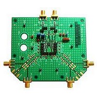
... LNA inputs, outputs, and gain setting pins. The board is shipped in a typical G = 12.04 dB configuration but is designed to allow customization of the setup as required. The AD8432-EVALZ requires a single 5 V power supply. An on-board switch (S1) allows VPS to drive the enable (ENB) input. GAIN SETTING ...
Page 26
... AD8432 SCHEMATIC GML1 19 12 GML2 20 11 GMH1 GMH2 10 GOH1 21 GOH2 OPH1 22 9 OPH2 VPS1 23 8 VPS2 7 ENB 24 IND2 Figure 74. Schematic Rev Page 08341-042 ...
Page 27
... POWER SUPPLY The AD8432 should be powered by a single 5 V supply connected to the VPOS terminal. Separate supplies can be used for VPS1, VPS2, and ENB, or they can all be tied to VPOS by shorting the W3 and W4 headers and the S1 switch. Ferrite beads and decoupling capacitors are installed for isolation, protection, and power supply noise reduction ...
Page 28
... Temperature Range AD8432ACPZ-R7 −40°C to +85°C AD8432ACPZ-RL −40°C to +85°C AD8432ACPZ-WP −40°C to +85°C AD8432-EVALZ RoHS Compliant Part. ©2009-2011 Analog Devices, Inc. All rights reserved. Trademarks and registered trademarks are the property of their respective owners. 4.10 0.30 4.00 SQ ...