CY3218-CAPEXP1 Cypress Semiconductor Corp, CY3218-CAPEXP1 Datasheet - Page 23
CY3218-CAPEXP1
Manufacturer Part Number
CY3218-CAPEXP1
Description
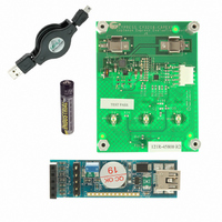
KIT CAPSENSE EXPRESS CY8C20110
Manufacturer
Cypress Semiconductor Corp
Series
CapSense Express™r
Specifications of CY3218-CAPEXP1
Sensor Type
Touch, Capacitive
Interface
I²C, USB
Voltage - Supply
0.9 V ~ 1.5 V
Embedded
Yes, Other
Utilized Ic / Part
CY8C20110
Processor To Be Evaluated
CY8C201x
Lead Free Status / RoHS Status
Lead free / RoHS Compliant
Sensitivity
-
Sensing Range
-
Lead Free Status / Rohs Status
Lead free / RoHS Compliant
Other names
428-2043
Available stocks
Company
Part Number
Manufacturer
Quantity
Price
Company:

Part Number:
CY3218-CAPEXP1
Manufacturer:
CYPRESS
Quantity:
15


DC Electrical Characteristics
DC Chip Level Specifications
DC GPIO Specifications
Table 7. 5-V and 3.3-V DC GPIO Specifications
This table lists guaranteed maximum and minimum specifications for the voltage and temperature ranges: 4.75 V to 5.25 V and
–40 °C < T
guidance only.
Document Number: 001-54606 Rev. *E
V
I
ISB
ISB
ISB
V
V
V
V
V
I
I
I
V
V
V
V
V
I
C
C
Parameter
Parameter
DD
OH1
OH2
OL
IL
DD
OH1
OH2
OH3
OH4
OL
IL
IH
IL
IH
H
IN
OUT
A
< 85 °C, 3.10 V to 3.6 V and –40 °C < T
Supply voltage
Supply current
Deep sleep mode current with POR
and LVD active
Deep sleep mode current with POR
and LVD active
Deep sleep mode current with POR
and LVD active
High output voltage on Port 0 pins
High output voltage on Port 0 pins
High output voltage on Port 1 pins
High output voltage on Port 1 pins
Low output voltage
High output current on Port 0 pins
High output current on Port 1 pins
Low output current
Input low voltage
Input high voltage
Input low voltage
Input high voltage
Input hysteresis voltage
Input leakage
Capacitive load on pins as input
Capacitive load on pins as output
Description
Description
V
V
V
V
A
DD
DD
DD
DD
2.40
< 85 °C. Typical parameters apply to 5 V and 3.3 V at 25 °C and are for design
Min
0.01
0.01
Min
1.6
2.0
0.5
0.5
–
–
–
–
–
–
–
–
–
–
– 0.2
– 0.9
– 0.2
– 0.9
Typ
1.5
2.6
2.8
5.2
–
Typ
140
1.7
1.7
–
–
–
–
–
–
–
–
–
–
–
–
1
Max
5.25
2.5
6.4
Max
0.75
0.75
4
5
0.8
20
–
–
–
–
1
5
–
–
–
–
5
5
Unit
Unit
mA
mA
mA
mA
mV
µA
µA
µA
nA
pF
pF
V
V
V
V
V
V
V
V
V
V
Conditions are V
V
V
V
I
20 mA source current in all I/Os.
I
20 mA source current in all I/Os.
I
20 mA source current in all I/Os.
I
20 mA source current in all I/Os.
I
40/60 mA sink current on even port pins and
of 40/60 mA sink current on odd port
pins.
V
current in all IOs
V
current in all IOs
V
on pins P0_2, P1_2, P1_3, P1_4 and 60 mA
sink current on pins P0_0, P0_1, P0_3,
P0_4, P1_0, P1_1
V
V
V
V
–
Gross tested to 1 µA.
Package and pin dependent.
Temp = 25 °C.
Package and pin dependent.
Temp = 25 °C.
OH
OH
OH
OH
OL
DD
DD
DD
DD
DD
DD
DD
DD
DD
DD
CY8C20160, CY8C20140
CY8C20110, CY8C20180
= 20 mA/pin, V
< 10 µA, V
= 1 mA, V
< 10 µA, V
= 5 mA, V
= 2.55 V, 0 °C < TA < 40 °C
= 3.3 V, –40 °C < TA < 85 °C
= 5.25 V, –40 °C < TA < 85 °C
≥ 3.1 V, maximum of 60 mA sink current
[20]
≥ 3.1 V, maximum of 20 mA source
= 3.10 V to 3.6 V.
= 3.10 V to 3.6 V.
= 4.75 V to 5.25 V.
= 4.75 V to 5.25 V.
≥ 3.1 V, maximum of 20 mA source
DD
DD
DD
DD
DD
> 3.10 V, maximum of
> 3.10 V, maximum of
> 3.10 V, maximum of
> 3.10 V, maximum of
Notes
Notes
DD
= 3.10 V, T
> 3.10, maximum of
CY8C20142
Page 23 of 39
A
= 25 °C
[+] Feedback
Related parts for CY3218-CAPEXP1
Image
Part Number
Description
Manufacturer
Datasheet
Request
R

Part Number:
Description:
KIT CAPSENSE EXPRESS CY8C20142
Manufacturer:
Cypress Semiconductor Corp
Datasheet:

Part Number:
Description:
KIT CAPSENSE EXPRESS CY8C201A0
Manufacturer:
Cypress Semiconductor Corp
Datasheet:

Part Number:
Description:
Manufacturer:
Cypress Semiconductor Corp
Datasheet:
Part Number:
Description:
Manufacturer:
Cypress Semiconductor Corp
Datasheet:
Part Number:
Description:
Manufacturer:
Cypress Semiconductor Corp
Datasheet:
Part Number:
Description:
Manufacturer:
Cypress Semiconductor Corp
Datasheet:
Part Number:
Description:
Manufacturer:
Cypress Semiconductor Corp
Datasheet: