CY3218-CAPEXP1 Cypress Semiconductor Corp, CY3218-CAPEXP1 Datasheet - Page 8
CY3218-CAPEXP1
Manufacturer Part Number
CY3218-CAPEXP1
Description
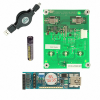
KIT CAPSENSE EXPRESS CY8C20110
Manufacturer
Cypress Semiconductor Corp
Series
CapSense Express™r
Specifications of CY3218-CAPEXP1
Sensor Type
Touch, Capacitive
Interface
I²C, USB
Voltage - Supply
0.9 V ~ 1.5 V
Embedded
Yes, Other
Utilized Ic / Part
CY8C20110
Processor To Be Evaluated
CY8C201x
Lead Free Status / RoHS Status
Lead free / RoHS Compliant
Sensitivity
-
Sensing Range
-
Lead Free Status / Rohs Status
Lead free / RoHS Compliant
Other names
428-2043
Available stocks
Company
Part Number
Manufacturer
Quantity
Price
Company:

Part Number:
CY3218-CAPEXP1
Manufacturer:
CYPRESS
Quantity:
15


I
The CapSense Express devices support the industry standard I
■
■
■
■
The I
I
The device uses a seven bit addressing protocol. The I
the first 7 bits contain the address and the LSB indicates the data transfer direction. Zero in the LSB bit indicates the write transaction
from master and one indicates read transfer by the master. The following table shows examples for different I
Table 4. I
I
‘Clock stretching’ or ‘bus stalling’ in I
is a state in which the slave holds the SCL line low to indicate
that it is busy. In this condition, the master is expected to wait till
the SCL is released by the slave.
When an I
device, the CapSense Express stalls the I
reception of each byte (that is, just before the ACK/NAK bit) until
processing of the byte is complete and critical internal functions
are executed. Use a fully I
with the CapSense Express device.
Document Number: 001-54606 Rev. *E
2
2
2
C Device Addressing
C Clock Stretching
Configuring the device
Reading the status and data registers of the device
Controlling device operation
Executing commands
C Interface
7-bit Slave
Address
2
C address can be modified during configuration.
75
75
1
1
2
2
C master communicates with the CapSense Express
C Address Examples
D7
0
0
1
1
2
C compliant master to communicate
D6
0
0
0
0
2
C communication protocol
D5
0
0
0
0
2
C bus after the
D4
0
0
1
1
D3
0
0
0
0
2
C data transfer is always initiated by the master sending a one byte address:
D2
0
0
1
1
2
C protocol, which can be used for:
If the I
software I
of time (as specified in
page 9) for each register write and read operation before the next
bit is transmitted. The I
should be high) before the I
with CapSense Express. If the master fails to do so and
continues to communicate, the communication is erroneous.
The following diagrams represent the ACK time delays shown in
“Format for Register Write and Read”
read.
D1
1
1
1
1
2
C master does not support clock stretching (a bit banged
0(W)
0(W)
1(W)
1(R)
2
D0
C Master), the master must wait for a specific amount
CY8C20160, CY8C20140
CY8C20110, CY8C20180
“Format for Register Write and Read”
2
C master must check the SCL status (it
2
C master initiates any data transfer
8-bit Slave Address
02
03
96
97
on page 9 for write and
2
C addresses.
CY8C20142
Page 8 of 39
on
[+] Feedback
Related parts for CY3218-CAPEXP1
Image
Part Number
Description
Manufacturer
Datasheet
Request
R

Part Number:
Description:
KIT CAPSENSE EXPRESS CY8C20142
Manufacturer:
Cypress Semiconductor Corp
Datasheet:

Part Number:
Description:
KIT CAPSENSE EXPRESS CY8C201A0
Manufacturer:
Cypress Semiconductor Corp
Datasheet:

Part Number:
Description:
Manufacturer:
Cypress Semiconductor Corp
Datasheet:
Part Number:
Description:
Manufacturer:
Cypress Semiconductor Corp
Datasheet:
Part Number:
Description:
Manufacturer:
Cypress Semiconductor Corp
Datasheet:
Part Number:
Description:
Manufacturer:
Cypress Semiconductor Corp
Datasheet:
Part Number:
Description:
Manufacturer:
Cypress Semiconductor Corp
Datasheet: