RD3803MMA7660FC Freescale Semiconductor, RD3803MMA7660FC Datasheet - Page 23
RD3803MMA7660FC
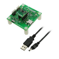
Manufacturer Part Number
RD3803MMA7660FC
Description
KIT EVAL BOARD MMA7660FC
Manufacturer
Freescale Semiconductor
Specifications of RD3803MMA7660FC
Sensor Type
Accelerometer, 3 Axis
Sensing Range
±1.5g
Interface
USB
Sensitivity
21.33 count/g
Voltage - Supply
5V, USB
Embedded
Yes, Other
Utilized Ic / Part
MMA7660
Acceleration
1.5 g
Sensing Axis
Triple Axis
Output Type
Digital
Interface Type
I2C
Operating Voltage
3.6 V
Operating Current
294 uA
Maximum Operating Temperature
+ 85 C
Minimum Operating Temperature
- 40 C
Lead Free Status / RoHS Status
Lead free / RoHS Compliant
Available stocks
Company
Part Number
Manufacturer
Quantity
Price
Company:

Part Number:
RD3803MMA7660FC
Manufacturer:
Freescale Semiconductor
Quantity:
135


Acknowledge
data. Thus each byte transferred effectively requires 9-bits. The master generates the 9
SDA during the acknowledge clock tap, such that the SDA line is stable low during the high period of the clock tap. When the
master is transmitting to MMA7660FC, it generates the acknowledge bit because it is the recipient. When the device is
transmitting to the master, the master generates the acknowledge bit because the master is the recipient.
The Slave Address
R/W bit, which is low for a write command and high for a read command. The device has a factory set I
is normally 1001100 (0x4C). Contact the factory to request a different I
to 1110111 (0x08 to 0xEF), by metal mask option.
recognizes its slave address, it acknowledges and is then ready for continued communication.
Message Format for Writing MMA7660FC
by at least one byte of information. The first byte of information is the register address of the first internal register that is to be
updated. The Master Write address is 1001 1000 (0x98). If a STOP condition is detected after just the register address is
received, then MMA7660FC takes no action. See
0x00 when a STOP condition is detected, so a single byte write has no net effect because the register address given in this first
and only byte is replaced by 0x00 at the STOP condition. The internal register address pointer is not, however, cleared on a
repeated start condition. Use a single byte write followed by a repeated start to read back data from a register.
selected by the register address. See
Sensors
Freescale Semiconductor
The acknowledge bit is a clocked 9th bit, shown in
MMA7660FC has a 7-bit long slave address, shown in
The device monitors the bus continuously, waiting for a START condition followed by its slave address. When the device
A write to MMA7660FC comprises the transmission of the device’s keyscan slave address with the R/W bit set to 0, followed
Any bytes received after the register address are data bytes. The first data byte goes into the internal register of the device
BY TRANSMITTER
BY RECEIVER
Master
Slave
SDA
SCL
SDA
SDA
SCL
ST
CONDITION
START
MSB
Device Address [6:0]
1
S
0
Figure
1
12.
0
W
Figure 12. Single Byte Write
Figure
Figure 11. Slave Address
Figure 10. Acknowledge
Figure
AK
1
12. MMA7660FC clears its internal register address pointer to register
Figure
2
10, which the recipient uses to handshake a receipt of each byte of
11. The bit following the 7-bit slave address (bit eight) is the
Register Address [6:0]
1
2
C slave address, which is available in the range 0001000
ACKNOWLEDGEMENT
0
CLOCK PULSE FOR
CLOCK TAP FOR
0
AK
th
8
clock tap, and the recipient pulls down
R/W
Data [7:0]
2
ACK
9
C slave address which
AK
MMA7660FC
SP
23
Related parts for RD3803MMA7660FC
Image
Part Number
Description
Manufacturer
Datasheet
Request
R

Part Number:
Description:
Manufacturer:
Freescale Semiconductor, Inc
Datasheet:
Part Number:
Description:
Manufacturer:
Freescale Semiconductor, Inc
Datasheet:
Part Number:
Description:
Manufacturer:
Freescale Semiconductor, Inc
Datasheet:
Part Number:
Description:
Manufacturer:
Freescale Semiconductor, Inc
Datasheet:
Part Number:
Description:
Manufacturer:
Freescale Semiconductor, Inc
Datasheet:
Part Number:
Description:
Manufacturer:
Freescale Semiconductor, Inc
Datasheet:
Part Number:
Description:
Manufacturer:
Freescale Semiconductor, Inc
Datasheet:
Part Number:
Description:
Manufacturer:
Freescale Semiconductor, Inc
Datasheet:
Part Number:
Description:
Manufacturer:
Freescale Semiconductor, Inc
Datasheet:
Part Number:
Description:
Manufacturer:
Freescale Semiconductor, Inc
Datasheet:
Part Number:
Description:
Manufacturer:
Freescale Semiconductor, Inc
Datasheet:
Part Number:
Description:
Manufacturer:
Freescale Semiconductor, Inc
Datasheet:
Part Number:
Description:
Manufacturer:
Freescale Semiconductor, Inc
Datasheet:
Part Number:
Description:
Manufacturer:
Freescale Semiconductor, Inc
Datasheet:
Part Number:
Description:
Manufacturer:
Freescale Semiconductor, Inc
Datasheet: