C8051F064EK Silicon Laboratories Inc, C8051F064EK Datasheet - Page 10
C8051F064EK
Manufacturer Part Number
C8051F064EK
Description
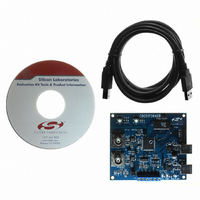
KIT EVAL FOR C8051F064
Manufacturer
Silicon Laboratories Inc
Type
MCUr
Specifications of C8051F064EK
Contents
Evaluation Board, Power Supply, USB Cables, Adapter and Documentation
Processor To Be Evaluated
C8051F06x
Interface Type
USB
Silicon Manufacturer
Silicon Labs
Core Architecture
8051
Silicon Core Number
C8051F064
Silicon Family Name
C8051F06x
Lead Free Status / RoHS Status
Contains lead / RoHS non-compliant
For Use With/related Products
C8051F064
Lead Free Status / Rohs Status
Lead free / RoHS Compliant
Other names
336-1219


C8051F064-EK
9.1. System Clock Sources
The C8051F064 device installed on the evaluation board features a calibrated programmable internal oscillator
that is enabled as the system clock source on reset. After reset, the internal oscillator operates at a frequency of
3.0625 MHz (±2%) by default but may be configured by software to operate at other frequencies. Therefore, in
many applications, an external oscillator is not required. However, an external 22.1184 MHz crystal is installed on
the evaluation board for additional applications. Refer to the C8051F06x data sheet for more information on
configuring the system clock source.
9.2. Switches and LEDs
Two switches are provided on the evaluation board. Switch SW1 is connected to the RESET pin of the C8051F064.
Pressing SW1 puts the device into its hardware-reset state. Switch SW2 is connected to the C8051F060’s general-
purpose I/O (GPIO) pin P3.7. Pressing SW2 generates a logic low signal on the port pin.
Four LEDs are also provided on the evaluation board.
9.3. DEBUG Interface (J1)
The evaluation board DEBUG USB port (J1) provides the interface between a PC USB port and the C8051F064’s
in-system debug/programming circuitry. In addition, this port is used for the ADC Demo detailed in Section 4.
Table 1 shows the DEBUG USB pin definitions.
9.4. DATA Interface (J7)
The evaluation board DATA USB port (J7) provides a data interface between a PC USB port and the CP2101
(Silicon Labs USB to UART bridge). This interface provides a virtual COM port via USB and will appear as a COM
port to PC applications.Table 2 shows the DATA USB pin definitions.
10
D1—The bi-color LED labeled “Run/Stop” indicates communications between the PC and the DEBUG USB port.
D2—The red LED D2 reflects the state of the SUSPEND signal of the DATA port device.
D3—The green LED labeled “P1.6” is connected to the C8051F064’s GPIO pin P1.6.
D4—The red LED labeled “PWR” indicates a power connection to the evaluation board.
Table 1. DEBUG USB Connector Pin Descriptions
Table 2. DATA USB Connector Pin Descriptions
Pin #
1
2
3
4
Pin #
1
2
3
4
Rev. 0.4
Description
Description
VBUS
GND
VBUS
GND
D–
D+
D–
D+
Related parts for C8051F064EK
Image
Part Number
Description
Manufacturer
Datasheet
Request
R

Part Number:
Description:
SMD/C°/SINGLE-ENDED OUTPUT SILICON OSCILLATOR
Manufacturer:
Silicon Laboratories Inc
Part Number:
Description:
Manufacturer:
Silicon Laboratories Inc
Datasheet:
Part Number:
Description:
N/A N/A/SI4010 AES KEYFOB DEMO WITH LCD RX
Manufacturer:
Silicon Laboratories Inc
Datasheet:
Part Number:
Description:
N/A N/A/SI4010 SIMPLIFIED KEY FOB DEMO WITH LED RX
Manufacturer:
Silicon Laboratories Inc
Datasheet:
Part Number:
Description:
N/A/-40 TO 85 OC/EZLINK MODULE; F930/4432 HIGH BAND (REV E/B1)
Manufacturer:
Silicon Laboratories Inc
Part Number:
Description:
EZLink Module; F930/4432 Low Band (rev e/B1)
Manufacturer:
Silicon Laboratories Inc
Part Number:
Description:
I°/4460 10 DBM RADIO TEST CARD 434 MHZ
Manufacturer:
Silicon Laboratories Inc
Part Number:
Description:
I°/4461 14 DBM RADIO TEST CARD 868 MHZ
Manufacturer:
Silicon Laboratories Inc
Part Number:
Description:
I°/4463 20 DBM RFSWITCH RADIO TEST CARD 460 MHZ
Manufacturer:
Silicon Laboratories Inc
Part Number:
Description:
I°/4463 20 DBM RADIO TEST CARD 868 MHZ
Manufacturer:
Silicon Laboratories Inc
Part Number:
Description:
I°/4463 27 DBM RADIO TEST CARD 868 MHZ
Manufacturer:
Silicon Laboratories Inc
Part Number:
Description:
I°/4463 SKYWORKS 30 DBM RADIO TEST CARD 915 MHZ
Manufacturer:
Silicon Laboratories Inc
Part Number:
Description:
N/A N/A/-40 TO 85 OC/4463 RFMD 30 DBM RADIO TEST CARD 915 MHZ
Manufacturer:
Silicon Laboratories Inc
Part Number:
Description:
I°/4463 20 DBM RADIO TEST CARD 169 MHZ
Manufacturer:
Silicon Laboratories Inc