C8051F064EK Silicon Laboratories Inc, C8051F064EK Datasheet - Page 11
C8051F064EK
Manufacturer Part Number
C8051F064EK
Description
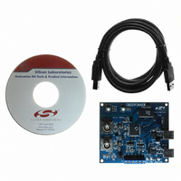
KIT EVAL FOR C8051F064
Manufacturer
Silicon Laboratories Inc
Type
MCUr
Specifications of C8051F064EK
Contents
Evaluation Board, Power Supply, USB Cables, Adapter and Documentation
Processor To Be Evaluated
C8051F06x
Interface Type
USB
Silicon Manufacturer
Silicon Labs
Core Architecture
8051
Silicon Core Number
C8051F064
Silicon Family Name
C8051F06x
Lead Free Status / RoHS Status
Contains lead / RoHS non-compliant
For Use With/related Products
C8051F064
Lead Free Status / Rohs Status
Lead free / RoHS Compliant
Other names
336-1219


9.5. Analog Inputs (J4, J5, J6, J8, J16, ADC0 [J13], ADC1 [J12])
Two BNC connectors (J13 (ADC0) and J12 (ADC1)) are provided on the C8051F064 board for easy evaluation of
the 16-bit on-chip ADCs. These analog inputs can be used to input an ac analog signal to the ADCs, ADC0 and
ADC1. Additionally, front-end circuitry is provided to condition the analog signals. To use this circuitry, follow the
guidelines listed below in conjunction with the schematic located in Section 10. See "AN190: Understanding ADC
Specifications" for a detailed discussion of issues related to ADC performance.
9.6. Analog I/O (Terminal Block [J3])
J3 is used to provide off-board voltage supply and voltage references for better noise performance evaluation in a
lab environment. Refer to Table 3 for terminal block connections.
Select the 5 V supply voltage for the Voltage References U3 and U6 at header J4. Place a shorting block on J4,
Pin 1 and Pin 2, to select the DATA VBUS signal. Place a shorting block on J4, Pin 2 and Pin 3, to select the
DEBUG VBUS signal.
A single-supply voltage option is provided on the evaluation board for the op-amps. Place a shorting block on J6
to connect the "V+" op-amp supply to AV+. Additionally, place a shorting block on J8 to connect the "V–"
op-amp supply to GND.
Provide a dual-supply voltage to the op-amps for optimal performance by removing the shorting blocks on
headers J6 and J8. To supply the voltages, +5 V and –5 V signals will need to be provided at the J3 terminal
block (Pin 1 and Pin 2).
Provide an external Conversion Start signal to ADC0 at header J5 Pin 1.
Provide an external Conversion Start signal to ADC1 at header J5 Pin 2.
Differential measurement from one test source: input signal to ADC0 and place shorting block on header J16.
Note:Remove shorting blocks from J6 and J8 BEFORE applying voltages to the J3 terminal block. Voltages applied to J3
while shorting blocks are on J6 and J8 could cause damage to the evaluation board.
Table 3. Terminal Block (J3) Pin Descriptions
Pin #
1
2
3
4
5
6
Rev. 0.4
Description
+3.3 VIN
AGND
5VDD
GND
–5 V
+5 V
C8051F064-EK
11
Related parts for C8051F064EK
Image
Part Number
Description
Manufacturer
Datasheet
Request
R

Part Number:
Description:
SMD/C°/SINGLE-ENDED OUTPUT SILICON OSCILLATOR
Manufacturer:
Silicon Laboratories Inc
Part Number:
Description:
Manufacturer:
Silicon Laboratories Inc
Datasheet:
Part Number:
Description:
N/A N/A/SI4010 AES KEYFOB DEMO WITH LCD RX
Manufacturer:
Silicon Laboratories Inc
Datasheet:
Part Number:
Description:
N/A N/A/SI4010 SIMPLIFIED KEY FOB DEMO WITH LED RX
Manufacturer:
Silicon Laboratories Inc
Datasheet:
Part Number:
Description:
N/A/-40 TO 85 OC/EZLINK MODULE; F930/4432 HIGH BAND (REV E/B1)
Manufacturer:
Silicon Laboratories Inc
Part Number:
Description:
EZLink Module; F930/4432 Low Band (rev e/B1)
Manufacturer:
Silicon Laboratories Inc
Part Number:
Description:
I°/4460 10 DBM RADIO TEST CARD 434 MHZ
Manufacturer:
Silicon Laboratories Inc
Part Number:
Description:
I°/4461 14 DBM RADIO TEST CARD 868 MHZ
Manufacturer:
Silicon Laboratories Inc
Part Number:
Description:
I°/4463 20 DBM RFSWITCH RADIO TEST CARD 460 MHZ
Manufacturer:
Silicon Laboratories Inc
Part Number:
Description:
I°/4463 20 DBM RADIO TEST CARD 868 MHZ
Manufacturer:
Silicon Laboratories Inc
Part Number:
Description:
I°/4463 27 DBM RADIO TEST CARD 868 MHZ
Manufacturer:
Silicon Laboratories Inc
Part Number:
Description:
I°/4463 SKYWORKS 30 DBM RADIO TEST CARD 915 MHZ
Manufacturer:
Silicon Laboratories Inc
Part Number:
Description:
N/A N/A/-40 TO 85 OC/4463 RFMD 30 DBM RADIO TEST CARD 915 MHZ
Manufacturer:
Silicon Laboratories Inc
Part Number:
Description:
I°/4463 20 DBM RADIO TEST CARD 169 MHZ
Manufacturer:
Silicon Laboratories Inc