C8051F064EK Silicon Laboratories Inc, C8051F064EK Datasheet - Page 2
C8051F064EK
Manufacturer Part Number
C8051F064EK
Description
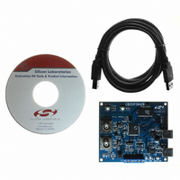
KIT EVAL FOR C8051F064
Manufacturer
Silicon Laboratories Inc
Type
MCUr
Specifications of C8051F064EK
Contents
Evaluation Board, Power Supply, USB Cables, Adapter and Documentation
Processor To Be Evaluated
C8051F06x
Interface Type
USB
Silicon Manufacturer
Silicon Labs
Core Architecture
8051
Silicon Core Number
C8051F064
Silicon Family Name
C8051F06x
Lead Free Status / RoHS Status
Contains lead / RoHS non-compliant
For Use With/related Products
C8051F064
Lead Free Status / Rohs Status
Lead free / RoHS Compliant
Other names
336-1219


C8051F064-EK
The C8051F064EK has three purposes:
4. Evaluation Kit ADC Demo
The C8051F064 evaluation kit includes a demonstration of the noise performance of the 16-bit ADCs on the
C8051F064 device. A 1.25 V dc input signal is provided on the board as an input to the ADC input pins, AIN0 and
AIN1. The ADCs convert and store 32,768 samples (differential, 16-bit samples in 2s complement) in off-chip
SRAM. The PC application then downloads the data through the debug USB port. After processing these
conversions, the software generates a spectral plot (magnitude versus frequency) of the ADC input signal. The
spectral plot illustrates the C8051F064s noise floor for the given sample set. The minimum and maximum values
sampled, mean of values sampled, standard deviation, and dynamic range are displayed. To run the ADC Demo,
first configure the evaluation board and install the PC application.
4.1. ADC Demo Hardware Setup
Configure the evaluation board according to the instructions below. A diagram of the final configuration is shown in
Figure 2. Configuration shorting blocks may already be installed.
2
Noise Performance Demonstration—Demonstrates 16-bit dc performance; displays FFT plot and key
parameters.
Performance Evaluation—Facilitates easy programming and analog front end input for dynamic performance
evaluation of ac signals.
Tools Test Drive—Allows easy evaluation of the Silicon Laboratories Integrated Development Environment
(IDE) (code download and on-chip debug function).
1. Place a shorting block on the J2 header connecting Pin 2 and Pin 3. This configures the evaluation board
2. Place a shorting block on the J4 header connecting Pin 2 and Pin 3. This configures the external voltage
3. Place shorting blocks on the "V+" (J6) and "V–" (J8) headers.
4. Configure SRAM(U5): Place shorting blocks on J11 and on J14 connecting Pin 2 and Pin 3.
5. Connect one end of the provided USB cable to any available USB port on the PC.
6. Connect the other end of the USB cable into the USB connector on the board labeled "DEBUG" (J1). This
to be powered from the DEBUG USB connector (J1).
reference to be powered from the DEBUG USB connector (J1).
connection should power the board. Evaluation board power is indicated by the "PWR" LED (D4).
ADC1
ADC0
J12
J13
RESET
V+
V-
J16
Figure 2. ADC Demo Hardware Setup
P3.6
J6
J8
J5
Pin 1
C8051
F064
Rev. 0.4
J3
P1.6 PWR
D3
J11
J4
SRAM
5VDD
J4
D4
Pin 1
Pin 1
STOP/RUN
J2
J14
+3.3V
D1
DEBUG
Pin 1
DATA
J15
D2
J1
J7
Pin 1
Pin 2
USB Cable
To PC
USB Port
Related parts for C8051F064EK
Image
Part Number
Description
Manufacturer
Datasheet
Request
R

Part Number:
Description:
SMD/C°/SINGLE-ENDED OUTPUT SILICON OSCILLATOR
Manufacturer:
Silicon Laboratories Inc
Part Number:
Description:
Manufacturer:
Silicon Laboratories Inc
Datasheet:
Part Number:
Description:
N/A N/A/SI4010 AES KEYFOB DEMO WITH LCD RX
Manufacturer:
Silicon Laboratories Inc
Datasheet:
Part Number:
Description:
N/A N/A/SI4010 SIMPLIFIED KEY FOB DEMO WITH LED RX
Manufacturer:
Silicon Laboratories Inc
Datasheet:
Part Number:
Description:
N/A/-40 TO 85 OC/EZLINK MODULE; F930/4432 HIGH BAND (REV E/B1)
Manufacturer:
Silicon Laboratories Inc
Part Number:
Description:
EZLink Module; F930/4432 Low Band (rev e/B1)
Manufacturer:
Silicon Laboratories Inc
Part Number:
Description:
I°/4460 10 DBM RADIO TEST CARD 434 MHZ
Manufacturer:
Silicon Laboratories Inc
Part Number:
Description:
I°/4461 14 DBM RADIO TEST CARD 868 MHZ
Manufacturer:
Silicon Laboratories Inc
Part Number:
Description:
I°/4463 20 DBM RFSWITCH RADIO TEST CARD 460 MHZ
Manufacturer:
Silicon Laboratories Inc
Part Number:
Description:
I°/4463 20 DBM RADIO TEST CARD 868 MHZ
Manufacturer:
Silicon Laboratories Inc
Part Number:
Description:
I°/4463 27 DBM RADIO TEST CARD 868 MHZ
Manufacturer:
Silicon Laboratories Inc
Part Number:
Description:
I°/4463 SKYWORKS 30 DBM RADIO TEST CARD 915 MHZ
Manufacturer:
Silicon Laboratories Inc
Part Number:
Description:
N/A N/A/-40 TO 85 OC/4463 RFMD 30 DBM RADIO TEST CARD 915 MHZ
Manufacturer:
Silicon Laboratories Inc
Part Number:
Description:
I°/4463 20 DBM RADIO TEST CARD 169 MHZ
Manufacturer:
Silicon Laboratories Inc