DM240312 Microchip Technology, DM240312 Datasheet - Page 35
DM240312
Manufacturer Part Number
DM240312
Description
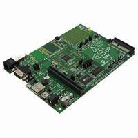
BOARD DEV PIC24FJ256DA210
Manufacturer
Microchip Technology
Series
dsPIC™r
Type
MCUr
Specifications of DM240312
Contents
Board
Processor To Be Evaluated
PIC24FJ256DA210
Data Bus Width
16 bit
Interface Type
RS-232, USB, Ethernet, SPI, UART
Operating Supply Voltage
9 V to 15 V
Silicon Manufacturer
Microchip
Core Architecture
PIC
Core Sub-architecture
PIC24
Silicon Core Number
PIC24F
Silicon Family Name
PIC24FJxxDAxxx
Kit Contents
Board
Lead Free Status / RoHS Status
Lead free / RoHS Compliant
For Use With/related Products
PIC24FJ256DA210
Lead Free Status / Rohs Status
Lead free / RoHS Compliant
Available stocks
Company
Part Number
Manufacturer
Quantity
Price
Company:

Part Number:
DM240312
Manufacturer:
Microchip Technology
Quantity:
135
Company:
Part Number:
DM240312
Manufacturer:
MICROCHIP
Quantity:
12 000


2010 Microchip Technology Inc.
Due to pin constraints, some features of the development board overlap more than oth-
ers. In these cases, configuring the board for one major functionality means limiting or
disabling another. Table 4-2 shows the major areas of overlap. Additional details are
provided in the following sections.
TABLE 4-2:
4.4.1
The PIC24FJ256DA210 Development Board implements a variety of user-defined
inputs: push button switches, capacitance-sensing touch pads, a potentiometer, and
four LEDs. The development board multiplexes the switches, touch sensors, potenti-
ometer and three of the LEDs through three I/O pins (RB5, RE9 and RG8). For each of
these pins, only one input mode can be chosen at any given time. The fourth LED (D4)
shares a pin with an address line for the external memory devices.
Note that the implementation of shared inputs and outputs used in the development
board is not a recommended design practice. In this case, it is implemented in consid-
eration of I/O pin constraints. Using separate pins for different input and output features
is always recommended.
If the CTMU touch sensors are enabled, the LEDs can be used simultaneously. How-
ever, care must be taken in the application to switch the I/O pins alternately as analog
input and digital output as required. Please refer to the “PIC24FJ256DA210 Family
Data Sheet” (DS39969) for details on configuring the I/O ports.
The user-defined features are configured using jumpers J13, J14 and J15. In some
cases, modifications to accompanying resistors are also required. The locations of the
components are shown in Figure 4-3. A summary of the jumper settings is provided in
Table 4-3.
Flash and SRAM
access modes
Parallel Flash/
SPI Flash Memory
SRAM
Resistive Touchscreen
OR Touch SPI channel
Potentiometer
Touch pads (CTMU)
User-defined Buttons
User-defined LEDs
UART Channels
USB Modes
PICtail Plus Expansion
Note 1:
Individual Feature
2:
3:
The only display mode available in this configuration is 16 bpp.
CTMU channels and push buttons are available with certain PICtail™ Daughter
Boards only. The number of inputs available depends on the daughter board and
the application. See Section 4.4.6 “PICtail™ Plus Card Modular Expansion
Connector” for additional information.
LED outputs are shared with CTMU input channels.
User-Defined Inputs and LEDs
SUMMARY OF BOARD CONFIGURATIONS VS. AVAILABILITY
OF SPECIFIC FEATURES
512 Kbytes/
512 Kbytes
No CTMU
Byte and
Host or
Device
2 Mbit
Word
Development Board Hardware
N
N
N
Y
Y
Y
1
512 Kbytes/
512 Kbytes
Byte and
Host or
Board Configuration Options
Device
CTMU
2 Mbit
Word
Y
Y
Y
N
N
Y
1
(2)
(3)
(3)
512 Kbytes/
512 Kbytes
USB OTG
OTG only
Byte and
2 Mbit
Word
Y
N
N
N
N
N
1
PICtail™ Plus Options
256 Kbytes/N.A.
Host or Device
Word only
256 Kbytes
DS51911A-page 35
Y
Y
N
Y
1
1
Y
(2)
(1)
Related parts for DM240312
Image
Part Number
Description
Manufacturer
Datasheet
Request
R

Part Number:
Description:
Manufacturer:
Microchip Technology Inc.
Datasheet:
Part Number:
Description:
Manufacturer:
Microchip Technology Inc.
Datasheet:
Part Number:
Description:
Manufacturer:
Microchip Technology Inc.
Datasheet:
Part Number:
Description:
Manufacturer:
Microchip Technology Inc.
Datasheet:
Part Number:
Description:
Manufacturer:
Microchip Technology Inc.
Datasheet:
Part Number:
Description:
Manufacturer:
Microchip Technology Inc.
Datasheet:
Part Number:
Description:
Manufacturer:
Microchip Technology Inc.
Datasheet:
Part Number:
Description:
Manufacturer:
Microchip Technology Inc.
Datasheet: