TOOLSTICK540DC Silicon Laboratories Inc, TOOLSTICK540DC Datasheet - Page 130
TOOLSTICK540DC
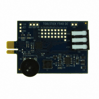
Manufacturer Part Number
TOOLSTICK540DC
Description
DAUGHTER CARD TOOLSTICK F540
Manufacturer
Silicon Laboratories Inc
Series
ToolStickr
Type
MCUr
Datasheets
1.TOOLSTICK540DC.pdf
(274 pages)
2.TOOLSTICK540DC.pdf
(16 pages)
3.TOOLSTICK540DC.pdf
(12 pages)
Specifications of TOOLSTICK540DC
Contents
Daughter Card
Processor To Be Evaluated
C8051F54x
Processor Series
C8051F54x
Interface Type
USB
Operating Supply Voltage
2.7 V to 3.6 V
Lead Free Status / RoHS Status
Lead free / RoHS Compliant
For Use With/related Products
C8051F54x
For Use With
336-1345 - TOOLSTICK BASE ADAPTER336-1182 - ADAPTER USB DEBUG FOR C8051FXXX
Lead Free Status / Rohs Status
Lead free / RoHS Compliant
Other names
336-1717


C8051F54x
16.1. Power-On Reset
During power-up, the device is held in a reset state and the RST pin is driven low until V
V
increases (V
power-on and V
On exit from a power-on reset, the PORSF flag (RSTSRC.1) is set by hardware to logic 1. When PORSF is
set, all of the other reset flags in the RSTSRC Register are indeterminate (PORSF is cleared by all other
resets). Since all resets cause program execution to begin at the same location (0x0000) software can
read the PORSF flag to determine if a power-up was the cause of reset. The content of internal data mem-
ory should be assumed to be undefined after a power-on reset. The V
power-on reset.
16.2. Power-Fail Reset/V
When a power-down transition or power irregularity causes V
monitor will drive the RST pin low and hold the CIP-51 in a reset state (see Figure 16.2). When V
to a level above V
memory contents are not altered by the power-fail reset, it is impossible to determine if V
the level required for data retention. If the PORSF flag reads 1, the data may no longer be valid. The V
monitor is enabled after power-on resets. Its defined state (enabled/disabled) is not altered by any other
reset source. For example, if the V
V
monitor must be enabled to the higher setting (VDMLVL = 1) and selected as a reset source if soft-
ware contains routines which erase or write Flash memory. If the V
set to the high level, any erase or write performed on Flash memory will cause a Flash Error device
reset.
130
RST
DD
. A delay occurs before the device is released from reset; the delay decreases as the V
monitor will still be disabled after the reset. To protect the integrity of Flash contents, the V
DD
DD
ramp time is defined as how fast V
Logic HIGH
Logic LOW
RST
monitor reset timing.
2.70
2.55
2.0
1.0
, the CIP-51 will be released from the reset state. Note that even though internal data
Figure 16.2. Power-On and V
/RST
DD
V
RST
DD
Monitor
monitor is disabled by code and a software reset is performed, the
Power-On
Reset
T
PORDelay
Rev. 1.1
DD
DD
ramps from 0 V to V
Monitor Reset Timing
DD
to drop below V
Monitor
Reset
VDD
DD
DD
monitor is enabled following a
monitor is not enabled and
RST
). Figure 16.2. plots the
RST
VDD
, the power supply
DD
DD
t
dropped below
settles above
DD
ramp time
DD
returns
DD
DD
Related parts for TOOLSTICK540DC
Image
Part Number
Description
Manufacturer
Datasheet
Request
R

Part Number:
Description:
KIT TOOL EVAL SYS IN A USB STICK
Manufacturer:
Silicon Laboratories Inc
Datasheet:

Part Number:
Description:
TOOLSTICK DEBUG ADAPTER
Manufacturer:
Silicon Laboratories Inc
Datasheet:

Part Number:
Description:
TOOLSTICK BASE ADAPTER
Manufacturer:
Silicon Laboratories Inc
Datasheet:

Part Number:
Description:
TOOLSTICK DAUGHTER CARD
Manufacturer:
Silicon Laboratories Inc
Datasheet:

Part Number:
Description:
TOOLSTICK DAUGHTER CARD
Manufacturer:
Silicon Laboratories Inc
Datasheet:

Part Number:
Description:
TOOLSTICK DAUGHTER CARD
Manufacturer:
Silicon Laboratories Inc
Datasheet:

Part Number:
Description:
TOOLSTICK PROGRAMMING ADAPTER
Manufacturer:
Silicon Laboratories Inc
Datasheet:

Part Number:
Description:
TOOLSTICK DAUGHTER CARD
Manufacturer:
Silicon Laboratories Inc
Datasheet:

Part Number:
Description:
KIT STARTER TOOLSTICK
Manufacturer:
Silicon Laboratories Inc
Datasheet:

Part Number:
Description:
KIT UNIVERSITY TOOLSTICK STARTER
Manufacturer:
Silicon Laboratories Inc
Datasheet:

Part Number:
Description:
DAUGHTER CARD TOOLSTICK F330
Manufacturer:
Silicon Laboratories Inc
Datasheet:

Part Number:
Description:
CARD DAUGHTER UNIVRSTY TOOLSTICK
Manufacturer:
Silicon Laboratories Inc
Datasheet:

Part Number:
Description:
DAUGHTER CARD TOOLSTICK F582
Manufacturer:
Silicon Laboratories Inc
Datasheet:

Part Number:
Description:
DAUGHTER CARD TOOLSTICK F500
Manufacturer:
Silicon Laboratories Inc
Datasheet:

Part Number:
Description:
DAUGHTER CARD TOOLSTICK F560
Manufacturer:
Silicon Laboratories Inc
Datasheet: